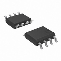
AP7168-SPG-13 Diodes Inc, AP7168-SPG-13 Datasheet - Page 8

AP7168-SPG-13
Manufacturer Part Number
AP7168-SPG-13
Description
IC REG LDO ADJ 1.2A 8SOP
Manufacturer
Diodes Inc
Datasheet
1.AP7168-SPG-13.pdf
(11 pages)
Specifications of AP7168-SPG-13
Regulator Topology
Positive Adjustable
Voltage - Output
0.8 ~ 5 V
Voltage - Input
2.2 ~ 5.5 V
Voltage - Dropout (typical)
0.5V @ 1A
Number Of Regulators
1
Current - Output
1.2A (Max)
Current - Limit (min)
1.2A
Operating Temperature
-40°C ~ 85°C
Mounting Type
Surface Mount
Package / Case
8-SOP
Input Voltage Max
5.5 V
Output Voltage
0.8 V to 5 V
Output Type
Adjustable
Dropout Voltage (max)
800 mV
Output Current
1.2 A
Line Regulation
0.02 %
Load Regulation
1.5 %
Voltage Regulation Accuracy
3 %
Maximum Power Dissipation
1.9 W
Maximum Operating Temperature
+ 85 C
Mounting Style
SMD/SMT
Minimum Operating Temperature
- 40 C
Lead Free Status / RoHS Status
Lead free / RoHS Compliant
Other names
AP7168-SPG-13DITR
Available stocks
Company
Part Number
Manufacturer
Quantity
Price
Company:
Part Number:
AP7168-SPG-13
Manufacturer:
DIODES
Quantity:
1 152
Company:
Part Number:
AP7168-SPG-13
Manufacturer:
ROHM
Quantity:
3 176
Application Note
No Load Stability
Other than external resistor divider, no minimum load is
required to keep the device stable. The device will remain
stable and regulated in no load condition.
ENABLE/SHUTDOWN Operation
The AP7168 is turned on by setting the EN pin high, and is
turned off by pulling it low. If this feature is not used, the
EN pin should be tied to IN pin to keep the regulator output
on at all time. To ensure proper operation, the signal
source used to drive the EN pin must be able to swing
above and below the specified turn-on/off voltage
thresholds listed in the Electrical Characteristics section
under V
POWER-OK
The Power-Ok (POK) pin is an active high open-drain
output. It can be connected to any 5.5V or lower rail
through an external pull-up resistor. The recommended
sink current of POK pin is up to 4mA, so the pull-up
resistor for POK should be in the range of 10kΩ to 1MΩ. If
output voltage monitoring is not needed, the POK pin can
be left floating.
Current Limit Protection
When output current at OUT pin is higher than current limit
threshold, the current limit protection will be triggered and
clamp the output current to approximately 1.6A (1.2A min)
to prevent over-current and to protect the regulator from
damage due to overheating.
Short Circuit Protection
When OUT pin is short-circuited to GND or OUT pin
voltage is less than 200mV, short circuit protection will be
triggered and clamp the output current to approximately
750mA. This feature protects the regulator from over-
current and damage due to overheating.
Low Quiescent Current
The AP7168, consuming only around 150µA for all input
range and output loading, provides great power saving in
portable and low power applications.
AP7168
Document number: DS32019 Rev. 2 - 2
IL
and V
IH
.
(Continued)
www.diodes.com
1.2A LOW DROPOUT REGULATOR WITH POK
8 of 11
Wide Output Range
The AP7168, with a wide output range of 0.8V to 5.0V,
provides a versatile solution for many portable and low
power applications.
Thermal Shutdown Protection
Thermal protection disables the output when the junction
temperature rises to approximately +145°C, allowing the
device to cool down. When the junction temperature
reduces to approximately +120°C the output circuitry is
enabled again. Depending on power dissipation, thermal
resistance,
protection circuit may cycle on and off. This cycling limits
the heat dissipation of the regulator, protecting it from
damage due to overheating.
Power Dissipation
The device power dissipation and proper sizing of the
thermal plane that is connected to the thermal pad is
critical to avoid thermal shutdown and ensuring reliable
operation. Power dissipation of the device depends on
input voltage and load conditions and can be calculated
by:
The AP7168 is available in the SO-8EP packages, both
with exposed pad, which is the primary conduction path for
heat to the printed circuit board (PCB). The pad can be
connected to ground or be left floating; however, to ensure
the device will not overheat, it should be attached to an
appropriate amount of copper PCB area.
However, the maximum power dissipation that can be
handled by the device depends on the maximum junction
to
temperature, and maximum device junction temperature,
which can be approximated by the equation below:
ambient
P
D
(max@
and
thermal
P
D
=
ambient
(
T
V
A
IN
resistance,
)
−
=
V
temperature,
(
OUT
+
150
)
R
xI
maximum
°
OUT
θ
C
AP7168
JA
© Diodes Incorporated
September 2010
−
T
the
A
)
ambient
thermal


