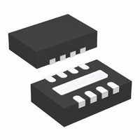
LT3080EDD#PBF Linear Technology, LT3080EDD#PBF Datasheet - Page 7

LT3080EDD#PBF
Manufacturer Part Number
LT3080EDD#PBF
Description
IC REG LDO ADJ 1.1A 8-DFN
Manufacturer
Linear Technology
Datasheet
1.LT3080ESTTRPBF.pdf
(26 pages)
Specifications of LT3080EDD#PBF
Regulator Topology
Positive Adjustable
Voltage - Output
0 ~ 36 V
Voltage - Input
1.2 ~ 36 V
Voltage - Dropout (typical)
1.35V @ 1.1A
Number Of Regulators
1
Current - Output
1.1A
Current - Limit (min)
1.1A
Operating Temperature
-40°C ~ 125°C
Mounting Type
Surface Mount
Package / Case
8-DFN
Voltage Regulator Type
Linear
Topology
LDO
Regulator Output Type
Adjustable
Polarity Type
Positive
Number Of Outputs
Single
Input Voltage (min)
1.2V
Input Voltage (max)
36V
Output Voltage
0 to 30V
Package Type
DFN EP
Output Current
1.1A
Load Regulation
1.3mV
Line Regulation
0.003mV/V
Operating Temp Range
-40C to 125C
Operating Temperature Classification
Automotive
Dropout Voltage@current (max)
0.2@100mA/0.5@1100mA
Pin Count
8
Mounting
Surface Mount
Quiescent Current (max)
1mA
Lead Free Status / RoHS Status
Lead free / RoHS Compliant
Available stocks
Company
Part Number
Manufacturer
Quantity
Price
TYPICAL PERFORMANCE CHARACTERISTICS
PIN FUNCTIONS
V
supply pin for the control circuitry of the device. The cur-
rent fl ow into this pin is about 1.7% of the output current.
For the device to regulate, this voltage must be more than
1.2V to 1.35V greater than the output voltage (see dropout
specifi cations).
IN (Pins 7, 8/Pins 7, 8/Pin 5/Pin 5/Pin 3): This is the
collector to the power device of the LT3080. The output
load current is supplied through this pin. For the device
to regulate, the voltage at this pin must be more than
0.1V to 0.5V greater than the output voltage (see dropout
specifi cations).
NC (Pin 6/Pin 6/Pin 1/Pin 1/NA): No Connection. No con-
nect pins have no connection to internal circuitry and may
be tied to V
CONTROL
(Pin 5/Pin 5/Pin 4/Pin 4/NA): This pin is the
IN
100μV/DIV
, V
CONTROL
V
OUT
Output Voltage Noise
V
R
C
C
I
LOAD
OUT
SET
OUT
SET
= O.1μF
= 100k
, V
= 1V
= 10μF
= 1.1A
OUT
(DD/MS8E/Q/T/ST)
, GND or fl oated.
TIME 1ms/DIV
3080 G26
OUT (Pins 1-3/Pins 1-3/Pin 3/Pin 3/Pin 2): This is the
power output of the device. There must be a minimum
load current of 1mA or the output may not regulate.
SET (Pin 4/Pin 4/Pin 2/Pin 2/Pin 1): This pin is the input
to the error amplifi er and the regulation set point for
the device. A fi xed current of 10μA fl ows out of this pin
through a single external resistor, which programs the
output voltage of the device. Output voltage range is zero
to the absolute maximum rated output voltage. Transient
performance can be improved by adding a small capacitor
from the SET pin to ground.
Exposed Pad (Pin 9/Pin 9/NA/NA/NA): OUT on MS8E and
DFN packages.
TAB: OUT on DD-Pak, TO-220 and SOT-223 packages.
–10
–15
–20
–25
–30
20
15
10
–5
5
0
10
Error Amplifi er Gain and Phase
100
FREQUENCY (Hz)
1k
10k
I
I
L
L
= 100mA
= 100mA
I
I
L
100k
L
= 1.1A
= 1.1A
3080 G28
1M
300
250
200
150
100
50
0
–50
–100
–150
–200
LT3080
3080fb
7


