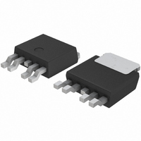
BD10KA5WFP-E2 Rohm Semiconductor, BD10KA5WFP-E2 Datasheet - Page 5

BD10KA5WFP-E2
Manufacturer Part Number
BD10KA5WFP-E2
Description
IC REG LDO 500MA 1.0V TO252-5
Manufacturer
Rohm Semiconductor
Datasheet
1.BD10KA5WFP-E2.pdf
(10 pages)
Specifications of BD10KA5WFP-E2
Regulator Topology
Positive Fixed
Voltage - Output
1V
Voltage - Input
2.3 ~ 5.5 V
Number Of Regulators
1
Current - Output
500mA (Max)
Operating Temperature
-40°C ~ 105°C
Mounting Type
Surface Mount
Package / Case
TO-252-4, DPak (4 Leads + Tab), TO-252AD
Number Of Outputs
1
Polarity
Positive
Input Voltage Max
5.5 V
Output Voltage
1 V
Output Type
Fixed
Output Current
500 mA
Line Regulation
35 mV
Load Regulation
75 mV
Voltage Regulation Accuracy
1 %
Maximum Power Dissipation
1.3 W
Maximum Operating Temperature
+ 105 C
Mounting Style
SMD/SMT
Minimum Operating Temperature
- 40 C
Lead Free Status / RoHS Status
Lead free / RoHS Compliant
Voltage - Dropout (typical)
-
Current - Limit (min)
-
Lead Free Status / Rohs Status
Lead free / RoHS Compliant
Other names
BD10KA5WFP-E2TR
Available stocks
Company
Part Number
Manufacturer
Quantity
Price
Part Number:
BD10KA5WFP-E2
Manufacturer:
ROHM/罗姆
Quantity:
20 000
●Input / Output Equivalent Circuit Diagrams
●Thermal Design
© 2009 ROHM Co., Ltd. All rights reserved.
BD□□KA5,BD□□KA5W Series,BD00KA5W Series
www.rohm.com
CTL
Vcc
2.0
1.6
1.2
0.8
0.4
0.0
When using at temperatures over Ta=25℃, please refer to the power dissipation shown in Fig.20 through 22.
The IC characteristics are closely related to the temperature at which the IC is used, so if the temperature exceeds the
maximum junction temperature Tj
consideration regarding instantaneous destruction and long-term operation reliability. In order to protect the IC from thermal
damage, it is necessary to operate it at temperatures less than the maximum junction temperature Tj
Even when the ambient temperature Ta is a normal temperature(25℃), the chip(junction) temperature Tj may be quite high,
so please operate the IC at temperatures less than the acceptable loss Pd.
The calculation method for power consumption Pc(W) is as follows :
It is then possible to find the maximum load current Io
Calculation Example
Example 1) When Ta=85℃, Vcc=2.5V, Vo=1.0V
Please refer to the above information and keep thermal designs within the scope of acceptable loss for all operating
temperature ranges.
The power consumption PC of the IC when there is a short circuit (short between Vo and GND) is :
0
1.30
Fig.20 Power Dissipation heat
Solving for the load current IO in order to operate within the acceptable loss,
Io≦
Io≦
Io≦440mA (Icca : 2mA)
Pc=Vcc×(Icca+Ishort)
reducing characteristics
25
Pc = (Vcc-Vo)×Io+Vcc×Icca
Acceptable loss Pd≧Pc
Ambient temperature:Ta(℃)
Pd – Vcc×Icca
0.676-2.5×Icca
Rohm standard board mounting
Board size:70×70×1.6mm
Copper foil area:7×7mm
θja=96.2(℃/W)
50
Vcc-Vo
Fig.18
TO252-5
2.5-1.0
75
31.25k Ω 2k Ω
100
25k Ω
2
125
*Ishort : Short circuit current
150
MAX,
Vcc Vcc
the device may malfunction or be destroyed. The heat of the IC requires sufficient
2.0
1.6
1.2
0.8
0.4
0.0
0
1.20
Fig.21 Power Dissipation heat
reducing characteristics
25
Ambient temperature:Ta(℃)
周囲温度:Ta(℃)
MAX
50
R2
R1
Rohm standard board mounting
Board size:70×70×1.6mm
Copper foil area:7×7mm
θja=104.2(℃/W)
BA10KA5WFP(TO252-5 packaging)
TO252-3
Vcc
with respect to the applied voltage Vcc at the time of thermal design.
θja=96.2℃/W → -10.4mW/℃
25℃=1300mW → 85℃=676mW
5/9
75
(BD00KA5WFP/WF)
100
Fig.19
OUT
ADJ
125
2
※ With BD00KA5WFP/WF,R1and R2 are connected
150
outside the IC between ADJ and GND and
between OUT and ADJ.
1000
800
600
400
200
0
0
Fig.22 Power Dissipation heat
687.6mW
562.6mW
reducing characteristics
Icca:
Vcc:
25
Vo:
Io:
Ambient temperature:Ta(℃)
周囲温度:Ta(℃)
Input voltage
Output voltage
Load current
Circuit current
50
(1)When using a standard board:
(2) When using an IC alone
SOP8
(1)
(2)
θj-c=181.8(℃/W)
θj-a=222.2(℃/W)
75
MAX.
Technical Note
2009.04 - Rev.A
100
125
150


