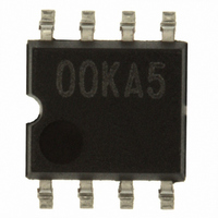
BD00KA5WF-E2 Rohm Semiconductor, BD00KA5WF-E2 Datasheet - Page 3

BD00KA5WF-E2
Manufacturer Part Number
BD00KA5WF-E2
Description
IC REG LDO 500MA ADJ SHTDN SOP8
Manufacturer
Rohm Semiconductor
Specifications of BD00KA5WF-E2
Regulator Topology
Positive Adjustable
Voltage - Output
1 ~ 4 V
Voltage - Input
2.3 ~ 5.5 V
Voltage - Dropout (typical)
0.12V @ 200mA
Number Of Regulators
1
Current - Output
500mA (Max)
Operating Temperature
-40°C ~ 105°C
Mounting Type
Surface Mount
Package / Case
8-SOP
Number Of Outputs
1
Polarity
Positive
Input Voltage Max
5.5 V
Output Voltage
1 V to 4 V
Output Type
Adjustable
Dropout Voltage (max)
0.2 V at 200 mA
Output Current
500 mA
Line Regulation
35 mV
Load Regulation
75 mV
Voltage Regulation Accuracy
1 %
Maximum Power Dissipation
0.6876 W
Maximum Operating Temperature
+ 105 C
Mounting Style
SMD/SMT
Minimum Operating Temperature
- 40 C
Reference Voltage
0.758 V
Lead Free Status / RoHS Status
Lead free / RoHS Compliant
Current - Limit (min)
-
Lead Free Status / Rohs Status
Lead free / RoHS Compliant
Other names
BD00KA5WF-E2TR
Available stocks
Company
Part Number
Manufacturer
Quantity
Price
Company:
Part Number:
BD00KA5WF-E2
Manufacturer:
TOSHIBA
Quantity:
3 000
●Reference Data (Unless specified otherwise, Vcc=25V,V
© 2009 ROHM Co., Ltd. All rights reserved.
BD□□KA5,BD□□KA5W Series,BD00KA5W Series
www.rohm.com
2.0
1.9
1.8
1.7
1.6
1.5
1.4
1.3
1.2
1.1
1.0
0.9
0.8
0.7
0.6
0.5
0.4
0.3
0.2
0.1
0.0
2.0
1.8
1.6
1.4
1.2
1.0
0.8
0.6
0.4
0.2
0.0
Fig.10 CTL Voltage vs. Output Voltage
1.6
1.6
1.6
1.5
1.5
1.5
1.5
1.5
1.4
1.4
1.4
-40
0.5
0.4
0.3
0.2
0.1
0.0
0.0
0.0 0.1 0.2 0.3 0.4 0.5 0.6 0.7 0.8 0.9 1.0 1.1 1.2 1.3 1.4 1.5
0.0
0.5
-20
0.5
Fig.7 Output Voltage
1.0
1.0
Fig.4 Load Stability
CONTROL VOLTAGE:VCTL[V]
OUTPUT CURRENT:IOUT[A]
1.5
0
Fig.1 Circuit current
(Io=5mA)
TEMPERATURE:Ta[ ℃ ]
SUPPLY VOLTAGE:VCC[V]
1.5
2.0
20
2.0
2.5
2.5
40
[BD15KA5WFP]
[BD15KA5WFP]
3.0
3.0
3.5
60
[BD15KA5WFP]
3.5
[BD15KA5WFP]
4.0
4.0
80
4.5
4.5
5.0
100
5.0
5.5
5.5
200
180
160
140
120
100
300
250
200
150
100
80
60
40
20
1.0
0.9
0.8
0.7
0.6
0.5
0.4
0.3
0.2
0.1
0.0
50
0
Fig.11 CTL Voltage vs. Output Current
2.0
1.8
1.6
1.4
1.2
1.0
0.8
0.6
0.4
0.2
0.0
0
0.0
-40
Fig.5 Input/Output Voltage Difference
0
0.0
0.5
Fig.8 Circuit Current
Temperature Characteristics
50
0.5
-20
1.0
100
1.0
CONTROL VOLTAGE:VCTL[V]
OUTPUT CURRENT:IOUT[mA]
(Vcc=3.135V)
1.5
0
Fig.2 Input Stability
150 200
TEMPERATURE :Ta[℃]
1.5
SUPPLY VOLTAGE:VCC[V]
(Io=0mA)
2.0
CTL
20
2.0
3/9
2.5
=2V,and Io=0mA)
[BD33KA5WFP]
2.5
250 300
3.0
40
[BD15KA5WFP]
3.0
[BD15KA5WFP]
3.5
60
3.5
350 400
[BD15KA5WFP]
4.0
4.0
80
4.5
4.5
5.0
450 500
100
5.0
5.5
5.5
60
55
50
45
40
35
30
25
20
15
10
5
0
10
2.0
1.9
1.8
1.7
1.6
1.5
1.4
1.3
1.2
1.1
1.0
0.9
0.8
0.7
0.6
0.5
0.4
0.3
0.2
0.1
0.0
2.0
1.8
1.6
1.4
1.2
1.0
0.8
0.6
0.4
0.2
0.0
8
6
4
2
0
100
10 15 20 25 30 35 40 45 50 55 60 65 70 75 80 85 90
0.0
0.0
Fig.12 Thermal Shutdown
Fig.9 Circuit Current by load Level
0.5
Circuit Characteristics (Io=5mA)
(ein=10dBV,Io=100mA)
Fig.6 Ripple Rejection
1.0
120
0.1
100
OUTPUT CURRENT:IOUT[A]
SUPPLY VOLTAGE:VCC[V]
Fig.3 Input Stability
1.5
(Io=500mA)
FREQUENCY:f[Hz]
TEMPERATURE:[ ℃]
2.0
140
0.2
2.5
Technical Note
2009.04 - Rev.A
1000
3.0
[BD15KA5WFP]
[BD15KA5WFP]
[BD15KA5WFP]
160
0.3
[BD15KA5WFP]
3.5
10000
4.0
180
0.4
4.5
5.0
100000
5.5
200
0.5


