LP2953AIM/NOPB National Semiconductor, LP2953AIM/NOPB Datasheet - Page 6
LP2953AIM/NOPB
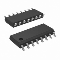
Manufacturer Part Number
LP2953AIM/NOPB
Description
IC REG LDO ADJ 250MA 16-SOIC
Manufacturer
National Semiconductor
Datasheet
1.LP2953IMNOPB.pdf
(22 pages)
Specifications of LP2953AIM/NOPB
Regulator Topology
Positive Adjustable
Voltage - Output
1.23 ~ 29 V
Voltage - Input
Up to 30V
Voltage - Dropout (typical)
0.47V @ 250mA
Number Of Regulators
1
Current - Output
250mA
Operating Temperature
-40°C ~ 125°C
Mounting Type
Surface Mount
Package / Case
16-SOIC (3.9mm Width)
Lead Free Status / RoHS Status
Lead free / RoHS Compliant
Current - Limit (min)
-
Other names
*LP2953AIM
*LP2953AIM/NOPB
LP2953AIM
*LP2953AIM/NOPB
LP2953AIM


www.national.com
All Voltage Options
Electrical Characteristics
Note 1: Absolute maximum ratings indicate limits beyond which damage to the component may occur. Electrical specifications do not apply when operating the
device outside of its rated operating conditions.
Note 2: The maximum allowable power dissipation is a function of the maximum junction temperature, T
and the ambient temperature, T
.
Exceeding the maximum allowable power dissipation will cause excessive die temperature, and the regulator will go into thermal shutdown. See APPLICATION
HINTS for additional information on heatsinking and thermal resistance.
Note 3: When used in dual-supply systems where the regulator load is returned to a negative supply, the output voltage must be diode-clamped to ground.
Note 4: May exceed the input supply voltage.
Note 5: Output or reference voltage temperature coefficient is defined as the worst case voltage change divided by the total temperature range.
Note 6: Load regulation is measured at constant junction temperature using low duty cycle pulse testing. Two separate tests are performed, one for the range of
100 µA to 1 mA and one for the 1 mA to 250 mA range. Changes in output voltage due to heating effects are covered by the thermal regulation specification.
Note 7: Dropout voltage is defined as the input to output differential at which the output voltage drops 100 mV below the value measured with a 1V differential. At
very low values of programmed output voltage, the input voltage minimum of 2V (2.3V over temperature) must be observed.
Note 8: Ground pin current is the regulator quiescent current. The total current drawn from the source is the sum of the ground pin current, output load current, and
current through the external resistive divider (if used).
Note 9: V
Note 10: Thermal regulation is the change in output voltage at a time T after a change in power dissipation, excluding load or line regulation effects. Specifications
are for a 200 mA load pulse at V
Note 11: Connect a 0.1 µF capacitor from the output to the feedback pin.
Note 12: V
Note 13: Two separate tests are performed, one covering 2.5V ≤ V
Note 14: Comparator thresholds are expressed in terms of a voltage differential at the Feedback terminal below the nominal reference voltage measured atV
V
Figure 4).
Note 15: Human body model, 200 pF discharged through 1.5 kΩ.
Note 16: Drive Shutdown pin with TTL or CMOS-low level to shut regulator OFF, high level to turn regulator ON.
Note 17: A military RETS specification is available upon request. For more information on military products, please refer to the Mil-Aero web page at
http://www.national.com/appinfo/milaero/index.html.
O
(NOM) + 1V. To express these thresholds in terms of output voltage change, multiply by the Error amplifier gain, which is V
SHUTDOWN
REF
≤ V
OUT
≤ 1.1V, V
≤ (V
IN
− 1V), 2.3V ≤ V
OUT
A
. The maximum allowable power dissipation at any ambient temperature is calculated using the equation for P(MAX),
IN
= V
= V
O
O
(NOM)+15V (3W pulse) for T = 10 ms.
(NOM).
(Continued)
IN
≤ 30V, 100 µA ≤ I
(Continued)
L
IN
≤ 250 mA.
≤ V
O
(NOM)+1V and the other test for V
6
J
(MAX), the junction-to-ambient thermal resistance, θ
O
(NOM)+1V ≤ V
IN
OUT
≤ 30V.
/V
REF
= (R1 + R2)/R2(refer to
J–A
IN
=
,
Related parts for LP2953AIM/NOPB
Image
Part Number
Description
Manufacturer
Datasheet
Request
R

Part Number:
Description:
Manufacturer:
National Semiconductor
Datasheet:

Part Number:
Description:
IC REG LDO 3.3V 250MA 16-SOIC
Manufacturer:
National Semiconductor
Datasheet:
Part Number:
Description:
National Semiconductor [8-Bit D/A Converter]
Manufacturer:
National Semiconductor
Datasheet:
Part Number:
Description:
National Semiconductor [Media Coprocessor]
Manufacturer:
National Semiconductor
Datasheet:
Part Number:
Description:
Digitally Controlled Tone and Volume Circuit with Stereo Audio Power Amplifier, Microphone Preamp Stage and National 3D Sound
Manufacturer:
National Semiconductor
Datasheet:
Part Number:
Description:
Digitally Controlled Tone and Volume Circuit with Stereo Audio Power Amplifier, Microphone Preamp Stage and National 3D Sound
Manufacturer:
National Semiconductor
Datasheet:
Part Number:
Description:
AC97 Rev 2 Codec with Sample Rate Conversion and National 3D Sound
Manufacturer:
National Semiconductor
Part Number:
Description:
Manufacturer:
National Semiconductor
Datasheet:
Part Number:
Description:
Manufacturer:
National Semiconductor
Datasheet:
Part Number:
Description:
General Purpose, Low Voltage, Low Power, Rail-to-Rail Output Operational Amplifiers
Manufacturer:
National Semiconductor
Datasheet:
Part Number:
Description:
8-bit 20 MSPS flash A/D converter.
Manufacturer:
National Semiconductor
Datasheet:
Part Number:
Description:
Low Noise Quad Operational Amplifier
Manufacturer:
National Semiconductor
Datasheet:
Part Number:
Description:
Quad Differential Line Receivers
Manufacturer:
National Semiconductor
Datasheet:
Part Number:
Description:
Quad High Speed Trapezoidal? Bus Transceiver
Manufacturer:
National Semiconductor
Datasheet: