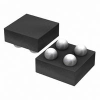
BH33RB1WGUT-E2 Rohm Semiconductor, BH33RB1WGUT-E2 Datasheet

BH33RB1WGUT-E2
Specifications of BH33RB1WGUT-E2
Related parts for BH33RB1WGUT-E2
BH33RB1WGUT-E2 Summary of contents
Page 1
CMOS LDO Regulators for Portable Equipments 1ch 150mA CMOS LDO Regulators BH□□RB1WGUT series ●Description The BH□□RB1WGUT series is a line of 150 mA output CMOS regulators that deliver a highly stable precision (± 1%) output voltage. Proprietary ROHM technology enables ...
Page 2
BH□□RB1WGUT series ●Absolute maximum ratings Parameter Applied supply voltage Power dissipation Operating temperature range Storage temperature range *1: Reduce by 5.3 mW/C over 25C, when mounted on a glass epoxy PCB (7 mm 0.8 mm). ●Recommended ...
Page 3
... Input Voltage VIN[V] Fig. 3 Output Voltage vs Input Voltage (BH33RB1WGUT Input Voltage VIN[V] Fig. 6 GND Current vs Input Voltage (BH33RB1WGUT) 3.5 3.0 2.5 2.0 1.5 1.0 0.5 0.0 0 100 200 300 400 Output Current IOUT[mA] Fig. 9 Output Voltage vs Output Current (BH33RB1WGUT) 2011.01 - Rev.C ...
Page 4
... Io=10mA 10 100 100 k 1M Frequency f[Hz] Fig. 17 Ripple Rejection (BH33RB1WGUT) IOUT = 1 mA → VOUT 50 mV/div 50 μs/div Fig, 20 Load Response (Co = 1.0 μF) (BH33RB1WGUT) 1 V/div STBY 1 V/div μ 3.3 kΩ 2.2 μF VOUT 100 μs/div Fig. 23 Output Voltage Rise Time (BH33RB1WGUT) 2011.01 - Rev.C ...
Page 5
BH□□RB1WGUT series ●Block Diagram, Recommended Circuit Diagram, and Pin Assignment Diagram BH□□RB1WGUT VIN VIN B2 VO LTAG ERE NCE Cin TH ERM ECT VER CU RRE ...
Page 6
BH□□RB1WGUT series ●Output capacitors Mounting input capacitor between input pin and GND (as close to pin as possible), and also output capacitor between output pin and GND(as close to pin as possible) is recommended. The input capacitor reduces the output ...
Page 7
BH□□RB1WGUT series 9. GND voltage The potential of GND pin must be minimum potential in all operating conditions. 10. Back Current In applications where the IC may be exposed to back current flow recommended to create a path ...
Page 8
BH□□RB1WGUT series ●Ordering part number Part No. Output voltage Series 15: 1.5 V RB1 : High ripple 18: 1.8 V 25: 2.5 V 28: 2.8 V 29: 2.9 V 30: 3.0 V 31: 3.1 V 33: ...
Page 9
No copying or reproduction of this document, in part or in whole, is permitted without the consent of ROHM Co.,Ltd. The content specified herein is subject to change for improvement without notice. The content specified herein is for the purpose ...


