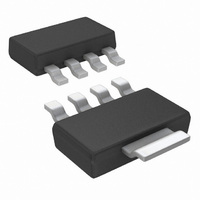
LP3964EMP-ADJ/NOPB National Semiconductor, LP3964EMP-ADJ/NOPB Datasheet - Page 14

LP3964EMP-ADJ/NOPB
Manufacturer Part Number
LP3964EMP-ADJ/NOPB
Description
IC REGULATOR ULTR LDO SOT223-5
Manufacturer
National Semiconductor
Datasheet
1.LP3961EMP-1.8NOPB.pdf
(22 pages)
Specifications of LP3964EMP-ADJ/NOPB
Regulator Topology
Positive Adjustable
Voltage - Output
1.2 ~ 5 V
Voltage - Input
2.5 ~ 7 V
Voltage - Dropout (typical)
0.24V @ 800mA
Number Of Regulators
1
Current - Output
800mA
Current - Limit (min)
1.2A
Operating Temperature
-40°C ~ 125°C
Mounting Type
Surface Mount
Package / Case
SOT-223 (4 leads + Tab)
Voltage Regulator Type
Linear
Topology
LDO
Regulator Output Type
Adjustable
Polarity Type
Positive
Number Of Outputs
Single
Input Voltage (min)
2.5V
Input Voltage (max)
7V
Output Voltage
1.2 to 5V
Package Type
SOT-223
Output Current
800mA
Load Regulation
0.02%
Line Regulation
0.02%
Output Voltage Accuracy
±1.5%
Operating Temp Range
-40C to 125C
Operating Temperature Classification
Automotive
Dropout Voltage@current (max)
0.03@80mA/0.3@800mA
Pin Count
4 +Tab
Mounting
Surface Mount
Lead Free Status / RoHS Status
Lead free / RoHS Compliant
Other names
LP3964EMP-ADJ
LP3964EMP-ADJTR
LP3964EMP-ADJTR
Available stocks
Company
Part Number
Manufacturer
Quantity
Price
Company:
Part Number:
LP3964EMP-ADJ/NOPB
Manufacturer:
TI
Quantity:
10 000
Company:
Part Number:
LP3964EMP-ADJ/NOPB
Manufacturer:
NS
Quantity:
2 000
www.national.com
Application Hints
Once the power pass element shuts down, the control loop
will rapidly cycle the output on and off until the average
power dissipation causes the thermal shutdown circuit to
respond to servo the on/off cycling to a lower frequency.
Please refer to the section on thermal information for power
dissipation calculations.
ERROR FLAG OPERATION
The LP3961/LP3964 produces a logic low signal at the Error
Flag pin when the output drops out of regulation due to low
input voltage, current limiting, or thermal limiting. This flag
has a built in hysteresis. The timing diagram in Figure 1
SENSE PIN
In applications where the regulator output is not very close to
the load, LP3964 can provide better remote load regulation
using the SENSE pin. Figure 2 depicts the advantage of the
SENSE option. LP3961 regulates the voltage at the output
pin. Hence, the voltage at the remote load will be the regu-
lator output voltage minus the drop across the trace resis-
(Continued)
FIGURE 1. Error Flag Operation
14
shows the relationship between the ERROR and the output
voltage. In this example, the input voltage is changed to
demonstrate the functionality of the Error Flag.
The internal Error flag comparator has an open drain output
stage. Hence, the ERROR pin should be pulled high through
a pull up resistor. Although the ERROR pin can sink current
of 1mA, this current is energy drain from the input supply.
Hence, the value of the pull up resistor should be in the
range of 100kΩ to 1MΩ. The ERROR pin must be con-
nected to ground if this function is not used. It should
also be noted that when the shutdown pin is pulled low, the
ERROR pin is forced to be invalid for reasons of saving
power in shutdown mode.
tance. For example, in the case of a 3.3V output, if the trace
resistance is 100mΩ, the voltage at the remote load will be
3.22V with 800mAmps of load current, I
regulates the voltage at the sense pin. Connecting the sense
pin to the remote load will provide regulation at the remote
load, as shown in Figure 2. If the sense option pin is not
required, the sense pin must be connected to the V
10112907
LOAD
. The LP3964
OUT
pin.


