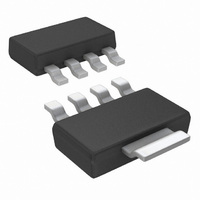
LP3964EMP-ADJ/NOPB National Semiconductor, LP3964EMP-ADJ/NOPB Datasheet - Page 7

LP3964EMP-ADJ/NOPB
Manufacturer Part Number
LP3964EMP-ADJ/NOPB
Description
IC REGULATOR ULTR LDO SOT223-5
Manufacturer
National Semiconductor
Datasheet
1.LP3961EMP-1.8NOPB.pdf
(22 pages)
Specifications of LP3964EMP-ADJ/NOPB
Regulator Topology
Positive Adjustable
Voltage - Output
1.2 ~ 5 V
Voltage - Input
2.5 ~ 7 V
Voltage - Dropout (typical)
0.24V @ 800mA
Number Of Regulators
1
Current - Output
800mA
Current - Limit (min)
1.2A
Operating Temperature
-40°C ~ 125°C
Mounting Type
Surface Mount
Package / Case
SOT-223 (4 leads + Tab)
Voltage Regulator Type
Linear
Topology
LDO
Regulator Output Type
Adjustable
Polarity Type
Positive
Number Of Outputs
Single
Input Voltage (min)
2.5V
Input Voltage (max)
7V
Output Voltage
1.2 to 5V
Package Type
SOT-223
Output Current
800mA
Load Regulation
0.02%
Line Regulation
0.02%
Output Voltage Accuracy
±1.5%
Operating Temp Range
-40C to 125C
Operating Temperature Classification
Automotive
Dropout Voltage@current (max)
0.03@80mA/0.3@800mA
Pin Count
4 +Tab
Mounting
Surface Mount
Lead Free Status / RoHS Status
Lead free / RoHS Compliant
Other names
LP3964EMP-ADJ
LP3964EMP-ADJTR
LP3964EMP-ADJTR
Available stocks
Company
Part Number
Manufacturer
Quantity
Price
Company:
Part Number:
LP3964EMP-ADJ/NOPB
Manufacturer:
TI
Quantity:
10 000
Company:
Part Number:
LP3964EMP-ADJ/NOPB
Manufacturer:
NS
Quantity:
2 000
SHORT CIRCUIT PROTECTION
OVER TEMPERATURE PROTECTION
SHUTDOWN INPUT
∆V
Absolute Maximum Ratings
If Military/Aerospace specified devices are required,
please contact the National Semiconductor Sales Office/
Distributors for availability and specifications.
Electrical Characteristics
LP3961/LP3964
V
Storage Temperature Range
Lead Temperature
ESD Rating (Note 3)
Power Dissipation (Note 2)
Input Supply Voltage (Survival)
Shutdown Input Voltage
(Survival)
Output Voltage (Survival), (Note
6), (Note 7)
Limits in standard typeface are for T
Unless otherwise specified: V
Symbol
IN
Tsh(h)
∆V
Tsh(t)
O
I
(Soldering, 5 sec.)
V
V
I
I
O(PK)
GND
GND
I
V
/ ∆I
- V
SDT
ADJ
SC
O
OL
OUT
OUT
Output Voltage
Tolerance
(Note 8)
Adjust Pin Voltage (ADJ
version)
Output Voltage Line
Regulation (Note 8)
Output Voltage Load
Regulation
(Note 8)
Ground Pin Current In
Normal Operation Mode
Ground Pin Current In
Shutdown Mode
(Note 11)
Peak Output Current
Short Circuit Current
Shutdown Threshold
Thermal Shutdown
Hysteresis
Shutdown Threshold
Dropout Voltage
Parameter
(Note 10)
IN
= V
O(NOM)
J
= 25˚C, and limits in boldface type apply over the full operating temperature range.
−0.3V to V
Internally Limited
−65˚C to +150˚C
−0.3V to +7.5V
−0.3V to +7.5V
+ 1V, I
10 mA ≤ I
V
10 mA ≤ I
V
V
10 mA
I
I
I
I
V
(Note 2)
Output = High
Output = Low
L
L
L
L
(Note 1)
OUT
OUT
OUT
SD
= 80 mA
= 800 mA
= 80 mA
= 800 mA
L
IN
≤ 0.2V
+1V
+1 ≤ V
+1.5V ≤ V
260˚C
= 10 mA, C
+0.3V
Conditions
<
2 kV
<
L
L
I
L
V
≤ 800mA
≤ 800mA
<
IN
IN
<
≤ 7.0V
800 mA
IN
7.0V
7
OUT
≤ 7.0V
Operating Ratings
I
Maximum Voltage for ERROR
Pin
Maximum Voltage for SENSE Pin
Input Supply Voltage (Operating),
(Note 12)
Shutdown Input Voltage
(Operating)
Maximum Operating Current (DC)
Operating Junction Temp. Range
OUT
= 33µF, V
(Survival)
(Note 4)
SD
1.216
0.02
0.06
0.02
0.08
Typ
240
165
1.5
2.8
V
24
15
10
0
3
4
0
= V
IN
IN
-0.3V.
V
1.198
1.180
LP3961/4 (Note 5)
IN
Min
-1.5
-3.0
1.2
1.1
–0.3
Short Circuit Protected
1.234
1.253
Max
+1.5
+3.0
300
350
0.2
−0.3V to V
30
35
10
14
15
25
75
9
−40˚C to +125˚C
2.5V to 7.0V
V
www.national.com
OUT
V
IN
IN
Units
+0.3V
+0.3V
+0.3V
mV
mA
µA
0.8A
˚C
˚C
%
%
%
V
A
A
V


