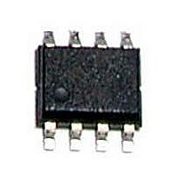
BD3951F-E2 Rohm Semiconductor, BD3951F-E2 Datasheet

BD3951F-E2
Specifications of BD3951F-E2
Available stocks
Related parts for BD3951F-E2
BD3951F-E2 Summary of contents
Page 1
... BD3951F ●Description BD3951F LDO system regulator particularly developed for automotive applications. The output current of the regulator can be drawn up to 150mA, and it has built-in power-on reset and input voltage sense. This device can withstand 50V surge input voltage as well as wide ambient temperature operations from -40℃ to +125℃. The adjustable reset delay time and detection input voltage allow to meet with wide range of design requirements. ● ...
Page 2
... BD3951F ●Electrical Characteristics(Unless otherwise specified Ta=-40℃~+125℃,Vcc=13.5V) Parameter Symbol [Whole Device] Input Current Icc [Regulator Block] Output Voltage Vout Line Regulation Lin.Reg Load Regulation Load.Reg Dropout Voltage ΔVd Output Peak Current Iomax [Reset Block] Threshold Voltage ...
Page 3
... BD3951F ●Reference Data(Unless otherwise specified Ta=-40℃~+125℃,Vcc=13.5V) -40℃ 25℃ 125℃ SUPPLY VOLTAGE: Vcc [V] Fig.1 Circuit Current 1 *Vcc=4.75V 0.8 0.6 125℃ 0.4 25℃ -40℃ 0 100 OUTPUT CURRENT: IOUT [mA] Fig.4 Drop Out Voltage 0.4 *Vcc=OUT=4.0V ...
Page 4
... BD3951F ●Block Diagram, Application Circuit, Pin Description Vcc 1 PreReg 0.33μF Vref R2:36kΩ R1:10kΩ VCC RADJ 3 VCC 2 SIN GND 5 Fig.13 ESR range of the output capacitor (ceramic capacitor) to 100Ω. ・ VCC must be more than 5V under the condition SIN is used for VCC voltage drop detection. ...
Page 5
... BD3951F ●Input/Output terminal Circuit SIN(2pin) Vcc 200k SIN(2pin) RES(6pin) OUT(8pin) 20k RES(6pin) ●How to set RESET delay time using CT terminal capacitor There are three factors to define the RESET delay time TdLH. External capacitor value Cct of the CT terminal, internal charge resistor and internal reference voltage. RESET delay time is approximately described as below equation. ...
Page 6
... BD3951F ●Thermal Design 1000 800 687 600 400 200 0 Please consider about power dissipation de-rating curve for high temperature operations. IC characteristics receive great effect from operating ambient temperature. If junction temperature exceeds rating temperature (Tjmax), device might degrade or be demolished permanently. reliability.To prevent thermal destroy, IC must be operated under the condition that junction temperature is less than Tjmax. ...
Page 7
... Therefore physical safety guard, like fuse, is recommended to prevent unexpected extreme condition which might beyond absolute maximum ratings. 2. BD3951F can operate within the operating supply voltage range and operating temperature range. The Limits over the input voltage is not warranted, however electric characteristics curve in operating condition should be within the expected linearity. ...
Page 8
... BD3951F might be damaged from the exceed inflow current from the terminals to VCC (for instance, VCC is short to GND while the output capacitor is charging.). In those cases, VCC series diode (to prevent inflow current) or bypass diode (connected from terminals to VCC) should be used externally in an application ...
Page 9
... BD3951F ●Ordering part number Part No. Part No. 3951 SOP8 5.0±0.2 (MAX 5.35 include BURR) + 6° 4° −4° 0.595 0.17 S 0.1 S 1.27 0.42±0.1 www.rohm.com © 2009 ROHM Co., Ltd. All rights reserved Package F: SOP8 <Tape and Reel information> Tape Embossed carrier tape ...
Page 10
No copying or reproduction of this document, in part or in whole, is permitted without the consent of ROHM Co.,Ltd. The content specified herein is subject to change for improvement without notice. The content specified herein is for the purpose ...


