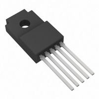
BA00CC0WT Rohm Semiconductor, BA00CC0WT Datasheet - Page 7

BA00CC0WT
Manufacturer Part Number
BA00CC0WT
Description
IC REG LDO 1A ADJ SHDN TO220FP-5
Manufacturer
Rohm Semiconductor
Datasheet
1.BA00CC0WCP-V5E2.pdf
(10 pages)
Specifications of BA00CC0WT
Regulator Topology
Positive Adjustable
Voltage - Output
Adjustable
Voltage - Input
4 ~ 25 V
Voltage - Dropout (typical)
0.3V @ 500mA
Number Of Regulators
1
Current - Output
1A (Max)
Operating Temperature
-40°C ~ 125°C
Mounting Type
Through Hole
Package / Case
TO-220-5 Full Pack (Straight Leads)
Number Of Outputs
1
Polarity
Positive
Input Voltage Max
25 V
Output Voltage
3 V to 15 V
Output Type
Adjustable
Dropout Voltage (max)
0.5 V at 500 mA
Output Current
1 A
Line Regulation
100 mV
Load Regulation
150 mV
Voltage Regulation Accuracy
2 %
Maximum Power Dissipation
2 W
Maximum Operating Temperature
+ 125 C
Mounting Style
Through Hole
Minimum Operating Temperature
- 40 C
Lead Free Status / RoHS Status
Lead free / RoHS Compliant
Current - Limit (min)
-
Lead Free Status / Rohs Status
Lead free / RoHS Compliant
Available stocks
Company
Part Number
Manufacturer
Quantity
Price
Part Number:
BA00CC0WT
Manufacturer:
ROMN
Quantity:
20 000
Part Number:
BA00CC0WT-V5/PB
Manufacturer:
ROHM/罗姆
Quantity:
20 000
BA00DD0WCP-V5,BA00DD0WHFP,BA00DD0WT,
BA00CC0WT,BA00CC0WT-V5,BA00CC0WCP-V5,BA00CC0WFP
●Vo Terminal
●Other
© 2011 ROHM Co., Ltd. All rights reserved.
www.rohm.com
Fig.33:Output equivalent circuit
IC
2) This IC is bipolar IC that has a P-board (substrate) and P+ isolation layer
Please attach an anti-oscillation capacitor between V
change due to factors such as temperature changes, which may cause oscillations. Please use a tantalum capacitor or
aluminum electrolytic capacitor with favorable characteristics and small external series resistance (ESR) even at low
temperatures. The output oscillates regardless of whether the ESR is large or small. Please use the IC within the stable
operating region while referring to the ESR characteristics reference data shown in Figs.33 through 35. In cases where there
are sudden load fluctuations, the a large capacitor is recommended.
1) Protection Circuits
Overcurrent Protection Circuit
Thermal Shutdown Circuit (Thermal Protection)
Reverse Current
A built-in overcurrent protection circuit corresponding to the current capacity prevents the destruction of the IC when there
are load shorts. This protection circuit is a “7”-shaped current control circuit that is designed such that the current is
restricted and does not latch even when a large current momentarily flows through the system with a high-capacitance
capacitor. However, while this protection circuit is effective for the prevention of destruction due to unexpected accidents, it
is not suitable for continuous operation or transient use. Please be aware when creating thermal designs that the overcurrent
protection circuit has negative current capacity characteristics with regard to temperature (Refer to Figs.4 and 16).
This system has a built-in temperature protection circuit for the purpose of protecting the IC from thermal damage. As
shown above, this must be used within the range of acceptable loss, but if the acceptable loss happens to be continuously
exceeded, the chip temperature Tj increases, causing the temperature protection circuit to operate.
When the thermal shutdown circuit operates, the operation of the circuit is suspended. The circuit resumes operation
immediately after the chip temperature Tj decreases, so the output repeats the ON and OFF states (Please refer to
Figs.12 and 24 for the temperatures at which the temperature protection circuit operates).
There are cases in which the IC is destroyed due to thermal runaway when it is left in the overloaded state. Be sure to
avoid leaving the IC in the overloaded state.
In order to prevent the destruction of the IC when a reverse current flows through the IC, it is recommended that a diode
be placed between the Vcc and Vo and a pathway be created so that the current can escape (Refer to Fig.36).
between each devise, as shown in Fig.37. A P-N junction is formed between
this P-layer and the N-layer of each device, and the P-N junction operates as a
parasitic diode when the electric potential relationship is GND> Terminal A,
GND> Terminal B, while it operates as a parasitic transistor when the electric
potential relationship is Terminal B GND> Terminal A. Parasitic devices are
intrinsic to the IC. The operation of parasitic devices induces mutual
interference between circuits, causing malfunctions and eventually the
destruction of the IC itself. It is necessary to be careful not to use the IC in ways
that would cause parasitic elements to operate. For example, applying a
voltage that is lower than the GND (P-board) to the input terminal.
N
(Pin B)
Parasitic element
or transistor
P+
O
Transistor (NPN)
B
OUT
E
N
N
P
GND
C(ADJ)
P
22 μ F
P+
Fig. 37: Example of the basic structure of a bipolar IC
N
100
GND
10
0.1
1
Fig.34:Io vs. ESR characteristics
0
(Pin A)
P
N
200
OUTPUT CURRENT:lo(mA)
P+
(BA□□CC0)
Stable operating region
Unstable operating region
400
Unstable operating region
Resistor
N
OUT
600
P
GND
Parasitic element
and GND. The capacitance of the capacitor may significantly
7/9
800
P+
1000
N
0.1
10
100
1
1
Fig.35: Io vs. ESR characteristics
(BA□□DD0)
(Pin B)
10
(Pin A)
Unstable operating region
OUTPUT CURRENT:lo(mA)
Stable operating region
B
Fig. 36:Bypass diode
C
E
CTL
GND
GND
Vcc
100
Parasitic element
Parasitic element
or transistor
Reverse current
Unstable operating region
GND
Technical Note
2011.03 - Rev.C
OUT
1000


