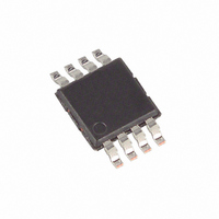
MAX1792EUA18+ Maxim Integrated Products, MAX1792EUA18+ Datasheet - Page 7

MAX1792EUA18+
Manufacturer Part Number
MAX1792EUA18+
Description
IC REG LDO 1.8V/ADJ 500MA 8-UMAX
Manufacturer
Maxim Integrated Products
Datasheet
1.MAX1792EUA15.pdf
(11 pages)
Specifications of MAX1792EUA18+
Regulator Topology
Positive Fixed or Adjustable
Voltage - Output
1.8V, 1.25 ~ 5 V
Voltage - Input
2.5 ~ 5.5 V
Number Of Regulators
1
Current - Output
500mA (Min)
Operating Temperature
-40°C ~ 85°C
Mounting Type
Surface Mount
Package / Case
8-MSOP, Micro8™, 8-uMAX, 8-uSOP,
Number Of Outputs
2
Polarity
Positive
Input Voltage Max
5.5 V
Output Voltage
1.25 V to 5 V, 1.8 V
Output Type
Adjustable, Fixed
Dropout Voltage (max)
360 mV
Output Current
500 mA
Line Regulation
0.15 %/V
Load Regulation
0.4 %
Voltage Regulation Accuracy
1.5 %
Maximum Power Dissipation
1.3 W
Maximum Operating Temperature
+ 85 C
Mounting Style
SMD/SMT
Minimum Operating Temperature
- 40 C
Reference Voltage
1.25 V
Lead Free Status / RoHS Status
Lead free / RoHS Compliant
Voltage - Dropout (typical)
-
Current - Limit (min)
-
Lead Free Status / Rohs Status
Lead free / RoHS Compliant
Figure 1. Functional Diagram
The MAX1792 is a low-dropout, low-quiescent-current
linear regulator designed primarily for battery-powered
applications. The device supplies loads up to 500mA
and is available with preset output voltages. As illustrat-
ed in Figure 1, the MAX1792 consists of a 1.25V refer-
ence, error amplifier, P-channel pass transistor, and
internal feedback voltage-divider.
The 1.25V reference is connected to the error amplifier,
which compares this reference with the feedback volt-
age and amplifies the difference. If the feedback volt-
age is lower than the reference voltage, the
pass-transistor gate is pulled lower, which allows more
current to pass to the output and increases the output
voltage. If the feedback voltage is too high, the pass-
transistor gate is pulled up, allowing less current to
pass to the output.
V
IN
VOLTAGE (V
= +2.5V TO +5.5V
ON
LOGIC SUPPLY
1μF
C
IN
OFF
OUT
μC
TO
)
R
100k
RST
_______________________________________________________________________________________
Detailed Description
SHDN
IN
IN
RST
MAX1792
SHUTDOWN
LOGIC
DELAY
TIMER
AMPLIFIER
93% V
ERROR
DRIVER WITH
Linear Regulator in µMAX
REF
MOSFET
I LIM
The output voltage is fed back through either an inter-
nal resistive divider connected to OUT or an external
resistor network connected to SET. The Dual Mode
comparator examines V
path. If V
is used and the output is regulated to the factory-preset
voltage.
Additional blocks include an output current limiter, ther-
mal sensor, and shutdown logic.
The MAX1792 features a 0.25Ω P-channel MOSFET
pass transistor. Unlike similar designs using PNP pass
transistors, P-channel MOSFETs require no base drive,
which reduces quiescent current. PNP-based regula-
tors also waste considerable current in dropout when
the pass transistor saturates, and use high base-drive
currents under large loads.
1.25V
V
REF
500mA Low-Dropout
THERMAL
SET
SENSOR
Internal P-Channel Pass Transistor
100mV
is below 50mV, the internal feedback path
5k
SET
GND
OUT
OUT
SET
and selects the feedback
V
OUT
= 1.25V TO 5.0V
R1
R2
C
3.3μF
OUT
7


