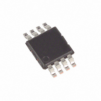
MAX1792EUA18+ Maxim Integrated Products, MAX1792EUA18+ Datasheet - Page 9

MAX1792EUA18+
Manufacturer Part Number
MAX1792EUA18+
Description
IC REG LDO 1.8V/ADJ 500MA 8-UMAX
Manufacturer
Maxim Integrated Products
Datasheet
1.MAX1792EUA15.pdf
(11 pages)
Specifications of MAX1792EUA18+
Regulator Topology
Positive Fixed or Adjustable
Voltage - Output
1.8V, 1.25 ~ 5 V
Voltage - Input
2.5 ~ 5.5 V
Number Of Regulators
1
Current - Output
500mA (Min)
Operating Temperature
-40°C ~ 85°C
Mounting Type
Surface Mount
Package / Case
8-MSOP, Micro8™, 8-uMAX, 8-uSOP,
Number Of Outputs
2
Polarity
Positive
Input Voltage Max
5.5 V
Output Voltage
1.25 V to 5 V, 1.8 V
Output Type
Adjustable, Fixed
Dropout Voltage (max)
360 mV
Output Current
500 mA
Line Regulation
0.15 %/V
Load Regulation
0.4 %
Voltage Regulation Accuracy
1.5 %
Maximum Power Dissipation
1.3 W
Maximum Operating Temperature
+ 85 C
Mounting Style
SMD/SMT
Minimum Operating Temperature
- 40 C
Reference Voltage
1.25 V
Lead Free Status / RoHS Status
Lead free / RoHS Compliant
Voltage - Dropout (typical)
-
Current - Limit (min)
-
Lead Free Status / Rohs Status
Lead free / RoHS Compliant
duction path from the die to the PC board. Additionally,
the MAX1792’s ground pin (GND) performs the dual
function of providing an electrical connection to system
ground and channeling heat away. Connect the
exposed backside pad and GND to the system ground
using a large pad or ground plane, or multiple vias to
the ground plane layer.
The MAX1792 delivers up to 0.5A
with input voltages up to 5.5V, but not simultaneously.
High output currents can only be sustained when input-
output differential voltages are low, as shown in Figure 3.
Capacitors are required at the MAX1792’s input and
output for stable operation over the full temperature
range and with load currents up to 500mA. Connect a
1µF capacitor between IN and ground and a 3.3µF low
equivalent series resistance (ESR) capacitor between
OUT and ground. For output voltages less than 2V, use
a 4.7µF low-ESR output capacitor. The input capacitor
(C
Reduce noise and improve load-transient response,
stability, and power-supply rejection by using larger
output capacitors such as 10µF.
The output capacitor’s (C
output noise. Use output capacitors with an ESR of
0.1Ω or less to ensure stability and optimum transient
Figure 3. Power Operating Regions: Maximum Output Current
vs. Supply Voltage
IN
0.5
0.4
0.3
0.7
0.6
0.2
0
0.1
) lowers the source impedance of the input supply.
0
CONTINUOUS CURRENT LIMIT
0.5
Applications Information
1.0
_______________________________________________________________________________________
INPUT-OUTPUT VOLTAGE DIFFERENTIAL (V)
1.5
T
A
OUT
and Regulator Stability
= +85°C
2.0
) ESR affects stability and
Capacitor Selection
POWER-μMAX PACKAGE OPERATING
2.5
(RMS)
REGION AT T
3.0
T
A
= +70°C
MAXIMUM SUPPLY
VOLTAGE LIMIT
(V
OUT
and operates
3.5
= 1.25V)
J(MAX)
T
A
= +150°C
4.0
= +50°C
4.5
Linear Regulator in µMAX
TRANSISTOR COUNT: 845
response. Surface-mount ceramic capacitors have very
low ESR and are commonly available in values up to
10µF. Connect C
as possible to minimize the impact of PC board trace
inductance.
The MAX1792 is designed to operate with low dropout
voltages and low quiescent currents in battery-powered
systems while still maintaining good noise, transient
response, and AC rejection. See the Typical Operating
Characteristics for a plot of Power-Supply Rejection
Ratio (PSRR) vs. Frequency. When operating from
noisy sources, improved supply-noise rejection and
transient response can be achieved by increasing the
values of the input and output bypass capacitors and
through passive filtering techniques.
The MAX1792 load-transient response graphs (see
Typical Operating Characteristics) show two compo-
nents of the output response: a DC shift from the output
impedance due to the load current change, and the
transient response. A typical transient response for a
step change in the load current from 5mA to 500mA is
18mV. Increasing the output capacitor’s value and
decreasing the ESR attenuates the overshoot.
A regulator’s minimum input-to-output voltage differen-
tial (dropout voltage) determines the lowest usable sup-
ply voltage. In battery-powered systems, this
determines the useful end-of-life battery voltage.
Because the MAX1792 uses a P-channel MOSFET pass
transistor, its dropout voltage is a function of drain-to-
source on-resistance (R
current (see Typical Operating Characteristics):
The MAX1792 ground current remains below 150µA in
dropout.
Note: The MAX1792 has an exposed thermal pad on
the bottom side of the package.
500mA Low-Dropout
Noise, PSRR, and Transient Response
V
DROPOUT
Input-Output (Dropout) Voltage
IN
= V
and C
IN
- V
DS(ON)
OUT
OUT
Chip Information
as close to the MAX1792
) multiplied by the load
= R
DS(ON)
x I
OUT
9


