TDA3602/N3,112 NXP Semiconductors, TDA3602/N3,112 Datasheet
TDA3602/N3,112
Specifications of TDA3602/N3,112
935083750112
TDA3602U


Related parts for TDA3602/N3,112


TDA3602/N3,112 Summary of contents
Page 1
DATA SHEET TDA3602 Multiple output voltage regulator Product specification File under Integrated Circuits, IC01 INTEGRATED CIRCUITS July 1994 ...
Page 2
Philips Semiconductors Multiple output voltage regulator FEATURES Two V state controlled regulators (REG1 and REG2) P Regulator 3 operates during load dump or thermal shutdown Multi-function control pin A back-up circuit for Regulator 3 via a single capacitor Supply voltage ...
Page 3
Philips Semiconductors Multiple output voltage regulator QUICK REFERENCE DATA SYMBOL PARAMETER Supply V positive supply voltage P operating Regulator 3 on jump start load dump; Regulator 3 on operating load dump; Regulator total quiescent current P T ...
Page 4
Philips Semiconductors Multiple output voltage regulator handbook, full pagewidth July 1994 4 Product specification TDA3602 ...
Page 5
Philips Semiconductors Multiple output voltage regulator PINNING SYMBOL PIN V 1 positive supply voltage P REG1 2 Regulator 1 output RESET 3 reset output V 4 state control input sc HOLD 5 hold output GND 6 ground REG3 7 Regulator ...
Page 6
Philips Semiconductors Multiple output voltage regulator When the device is in the on mode, it will switch back to the reset mode when V drops below 7.3 V. When V drops below 3 V, the device will return to the ...
Page 7
Philips Semiconductors Multiple output voltage regulator SYMBOL PARAMETER Schmitt triggers CHMITT TRIGGER FOR HOLD AND REGULATORS P2 V rising voltage threshold thr V falling voltage threshold thf V hysteresis EGULATOR CHMITT TRIGGER V ...
Page 8
Philips Semiconductors Multiple output voltage regulator SYMBOL PARAMETER Reset output V LOW level output voltage OL V HIGH level output voltage OH I LOW level output current OL I HIGH level output current OH Hold output V LOW level output ...
Page 9
Philips Semiconductors Multiple output voltage regulator SYMBOL PARAMETER Regulator unless otherwise specified) REG3 V output voltage REG3 V output voltage REGL3 I leakage output current LO1 V line regulation REG3 V load regulation REGL3 SVRR3 ...
Page 10
Philips Semiconductors Multiple output voltage regulator Table 1 State control pin. STATE REG3 (5 V) Coma LOW current Sleep LOW current Wake HIGH current Reset HIGH current On HIGH current Power on HIGH current Power off off handbook, full pagewidth ...
Page 11
Philips Semiconductors Multiple output voltage regulator handbook, full pagewidth REGULATOR 3 state control reset REGULATORS 1 and 2 hold Table 2 Logic table HOLD function. V SCHMITT TRIGGER ...
Page 12
Philips Semiconductors Multiple output voltage regulator handbook, halfpage (Regulators 1 and Fig.5 Foldback current protection off handbook, full pagewidth SW1 V P SW2 July 1994 QUALITY SPECIFICATION ...
Page 13
Philips Semiconductors Multiple output voltage regulator APPLICATION INFORMATION Noise Table 3 Noise at regulator outputs dependent on capacitive load ( REGULATOR (NOTE 1) REG 150 mA 800 V 2 100 mA 500 V ...
Page 14
Philips Semiconductors Multiple output voltage regulator retro - rack on / off SW1 > 220 F retro - rack battery C1 > 220 F 100 k on SW1 off SW2 July 1994 220 nF V ...
Page 15
Philips Semiconductors Multiple output voltage regulator handbook, full pagewidth RESET RESET- MODE = 1 SET OFF July 1994 SET OFF RESET- MODE = 0 READ KEY no KEY = SET Fig.9 Flow chart for high end ...
Page 16
Philips Semiconductors Multiple output voltage regulator handbook, full pagewidth July 1994 16 Product specification TDA3602 ...
Page 17
Philips Semiconductors Multiple output voltage regulator Example of a modern car radio design with the TDA3602 D ESIGN CONSIDERATIONS A modern car radio set meets the following design considerations: 1. Semi on/off logic. The radio set has to switch on/off ...
Page 18
Philips Semiconductors Multiple output voltage regulator handbook, full pagewidth July 1994 18 Product specification TDA3602 ...
Page 19
Philips Semiconductors Multiple output voltage regulator A reset by the hold function can only be created when the state control pin remains LOW. This is accomplished by means of transistor T1 when Port P0,0 is high ohmic. Because of resistors ...
Page 20
Philips Semiconductors Multiple output voltage regulator The timing diagram can only be understood after a thorough investigation of the flow charts (see section Flow chart semi on/off logic with security code). Furthermore short and long RESET pulses can be seen ...
Page 21
Philips Semiconductors Multiple output voltage regulator handbook, full pagewidth WAIT HOLD ? = SET FLAG ? = P0, 0 (in P0 (o) WAIT 10 ms ...
Page 22
Philips Semiconductors Multiple output voltage regulator handbook, full pagewidth July 1994 22 Product specification TDA3602 ...
Page 23
Philips Semiconductors Multiple output voltage regulator halfpage START P1 ( yes P0 yes input P1, Y ...
Page 24
Philips Semiconductors Multiple output voltage regulator ignition switch = open (set was on with ignition off) handbook, full pagewidth 2 P1. 1 P0. 1 P0. 2 REGULATORS 1 and 2 key scan cycle July 1994 ...
Page 25
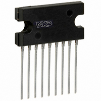
Philips Semiconductors Multiple output voltage regulator PACKAGE OUTLINE SIL9MPF: plastic single in-line medium power package with fin; 9 leads P pin 1 index DIMENSIONS (mm are the original dimensions UNIT ...
Page 26
Philips Semiconductors Multiple output voltage regulator SOLDERING Introduction There is no soldering method that is ideal for all IC packages. Wave soldering is often preferred when through-hole and surface mounted components are mixed on one printed-circuit board. However, wave soldering ...