NCV551SN50T1G ON Semiconductor, NCV551SN50T1G Datasheet - Page 4
NCV551SN50T1G
Manufacturer Part Number
NCV551SN50T1G
Description
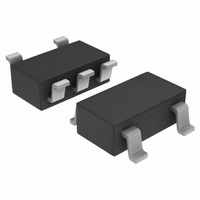
IC REG LDO 150MA 5.0V SOT23-5
Manufacturer
ON Semiconductor
Datasheet
1.NCP551SN29T1G.pdf
(11 pages)
Specifications of NCV551SN50T1G
Regulator Topology
Positive Fixed
Voltage - Output
5V
Voltage - Input
Up to 12V
Voltage - Dropout (typical)
0.04V @ 10mA
Number Of Regulators
1
Current - Output
150mA (Min)
Operating Temperature
-40°C ~ 125°C
Mounting Type
Surface Mount
Package / Case
TSOT-23-5, TSOT-5, TSOP-5
Number Of Outputs
1
Polarity
Positive
Input Voltage Max
12 V
Output Voltage
5 V
Output Type
Fixed
Dropout Voltage (max)
0.15 V at 10 mA
Output Current
150 mA
Line Regulation
30 mV
Load Regulation
65 mV
Voltage Regulation Accuracy
2 %
Maximum Operating Temperature
+ 125 C
Mounting Style
SMD/SMT
Minimum Operating Temperature
- 40 C
Lead Free Status / RoHS Status
Lead free / RoHS Compliant
Current - Limit (min)
-
Lead Free Status / Rohs Status
Lead free / RoHS Compliant
Other names
NCV551SN50T1G
NCV551SN50T1GOSTR
NCV551SN50T1GOSTR
Available stocks
Company
Part Number
Manufacturer
Quantity
Price
Company:

Part Number:
NCV551SN50T1G
Manufacturer:
ON
Quantity:
1 400
Company:
Part Number:
NCV551SN50T1G
Manufacturer:
ON Semiconductor
Quantity:
800
Part Number:
NCV551SN50T1G
Manufacturer:
ON/安森美
Quantity:
20 000


Load Regulation
current at a constant temperature.
Dropout Voltage
no longer maintains regulation against further reductions in
input voltage. Measured when the output drops 3% below its
nominal. The junction temperature, load current, and
minimum input supply requirements affect the dropout level.
Maximum Power Dissipation
will operate within its specifications.
Quiescent Current
the ground when the LDO operates without a load on its
output: internal IC operation, bias, etc. When the LDO
becomes loaded, this term is called the Ground current. It is
actually the difference between the input current (measured
through the LDO input pin) and the output current.
The change in output voltage for a change in output
The input/output differential at which the regulator output
The maximum total dissipation for which the regulator
The quiescent current is the current which flows through
http://onsemi.com
DEFINITIONS
4
Line Regulation
The measurement is made under conditions of low
dissipation or by using pulse technique such that the average
chip temperature is not significantly affected.
Line Transient Response
is excited with a given slope.
Thermal Protection
the integrated circuit in the event that the maximum junction
temperature is exceeded. When activated at typically 160°C,
the regulator turns off. This feature is provided to prevent
failures from accidental overheating.
Maximum Package Power Dissipation
dissipation level at which the junction temperature reaches
its maximum operating value, i.e. 125°C. Depending on the
ambient power dissipation and thus the maximum available
output current.
The change in output voltage for a change in input voltage.
Typical over and undershoot response when input voltage
Internal thermal shutdown circuitry is provided to protect
The maximum power package dissipation is the power
Related parts for NCV551SN50T1G
Image
Part Number
Description
Manufacturer
Datasheet
Request
R

Part Number:
Description:
ON Semiconductor [VOLTAGE REGULATOR]
Manufacturer:
ON Semiconductor
Datasheet:
Part Number:
Description:
357-036-542-201 CARDEDGE 36POS DL .156 BLK LOPRO
Manufacturer:
ON Semiconductor
Datasheet:
Part Number:
Description:
357-036-542-201 CARDEDGE 36POS DL .156 BLK LOPRO
Manufacturer:
ON Semiconductor
Datasheet:
Part Number:
Description:
357-036-542-201 CARDEDGE 36POS DL .156 BLK LOPRO
Manufacturer:
ON Semiconductor
Datasheet:
Part Number:
Description:
357-036-542-201 CARDEDGE 36POS DL .156 BLK LOPRO
Manufacturer:
ON Semiconductor
Datasheet:
Part Number:
Description:
357-036-542-201 CARDEDGE 36POS DL .156 BLK LOPRO
Manufacturer:
ON Semiconductor
Datasheet:
Part Number:
Description:
357-036-542-201 CARDEDGE 36POS DL .156 BLK LOPRO
Manufacturer:
ON Semiconductor
Datasheet:
Part Number:
Description:
357-036-542-201 CARDEDGE 36POS DL .156 BLK LOPRO
Manufacturer:
ON Semiconductor
Datasheet:
Part Number:
Description:
357-036-542-201 CARDEDGE 36POS DL .156 BLK LOPRO
Manufacturer:
ON Semiconductor
Datasheet:
Part Number:
Description:
357-036-542-201 CARDEDGE 36POS DL .156 BLK LOPRO
Manufacturer:
ON Semiconductor
Datasheet:
Part Number:
Description:
357-036-542-201 CARDEDGE 36POS DL .156 BLK LOPRO
Manufacturer:
ON Semiconductor
Datasheet:
Part Number:
Description:
Manufacturer:
ON Semiconductor
Datasheet:
Part Number:
Description:
Manufacturer:
ON Semiconductor
Datasheet:
Part Number:
Description:
Manufacturer:
ON Semiconductor
Datasheet: