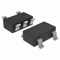
NCV551SN50T1G ON Semiconductor, NCV551SN50T1G Datasheet - Page 9

NCV551SN50T1G
Manufacturer Part Number
NCV551SN50T1G
Description
IC REG LDO 150MA 5.0V SOT23-5
Manufacturer
ON Semiconductor
Datasheet
1.NCP551SN29T1G.pdf
(11 pages)
Specifications of NCV551SN50T1G
Regulator Topology
Positive Fixed
Voltage - Output
5V
Voltage - Input
Up to 12V
Voltage - Dropout (typical)
0.04V @ 10mA
Number Of Regulators
1
Current - Output
150mA (Min)
Operating Temperature
-40°C ~ 125°C
Mounting Type
Surface Mount
Package / Case
TSOT-23-5, TSOT-5, TSOP-5
Number Of Outputs
1
Polarity
Positive
Input Voltage Max
12 V
Output Voltage
5 V
Output Type
Fixed
Dropout Voltage (max)
0.15 V at 10 mA
Output Current
150 mA
Line Regulation
30 mV
Load Regulation
65 mV
Voltage Regulation Accuracy
2 %
Maximum Operating Temperature
+ 125 C
Mounting Style
SMD/SMT
Minimum Operating Temperature
- 40 C
Lead Free Status / RoHS Status
Lead free / RoHS Compliant
Current - Limit (min)
-
Lead Free Status / Rohs Status
Lead free / RoHS Compliant
Other names
NCV551SN50T1G
NCV551SN50T1GOSTR
NCV551SN50T1GOSTR
Available stocks
Company
Part Number
Manufacturer
Quantity
Price
Company:
Part Number:
NCV551SN50T1G
Manufacturer:
ON
Quantity:
1 400
Company:
Part Number:
NCV551SN50T1G
Manufacturer:
ON Semiconductor
Quantity:
800
Part Number:
NCV551SN50T1G
Manufacturer:
ON/安森美
Quantity:
20 000
NOTE:
†For information on tape and reel specifications, including part orientation and tape sizes, please refer to our Tape and Reel Packaging Specific-
6. NCV551 is qualified for automotive use.
NCP551SN15T1
NCP551SN15T1G
NCP551SN18T1
NCP551SN18T1G
NCP551SN25T1
NCP551SN25T1G
NCP551SN27T1
NCP551SN27T1G
ORDERING INFORMATION
Enable
Input
ations Brochure, BRD8011/D.
The NCP551 series can be current boosted with a PNP transist-
or. Resistor R in conjunction with V
when the pass transistor begins conducting; this circuit is not
short circuit proof. Input/Output differential voltage minimum is
increased by V
If a delayed turn−on is needed during power up of several
voltages then the above schematic can be used. Resistor R,
and capacitor C, will delay the turn−on of the bottom regulator.
Input
1.0 mF
Additional voltages in 100 mV steps are available upon request by contacting your ON Semiconductor representative.
R
Device
Figure 21. Current Boost Regulator
R
Figure 23. Delayed Turn−on
BE
Q1
of the pass resistor.
1.0 mF
1.0 mF
C
1
2
3
1
2
3
1
2
3
Output Voltage
Nominal
BE
1.5
1.5
1.8
1.8
2.5
2.5
2.7
2.7
of the PNP determines
5
4
5
4
5
4
1.0 mF
1.0 mF
1.0 mF
Output
Output
Output
http://onsemi.com
Marking
Input
LAO
LAO
LAQ
LAQ
LAR
LAR
LAP
LAP
9
Input
1.0 mF
Q2
R
Short circuit current limit is essentially set by the V
R1. I
A regulated output can be achieved with input voltages that
exceed the 12 V maximum rating of the NCP551 series with
the addition of a simple pre−regulator circuit. Care must be
taken to prevent Q1 from overheating when the regulated
output (V
11 V
Figure 24. Input Voltages Greater than 12 V
SC
Figure 22. Current Boost Regulator with
= ((V
R1
R2
out
Q1
) is shorted to GND
BEQ2
1.0 mF
R3
(Pb−Free)
(Pb−Free)
(Pb−Free)
(Pb−Free)
− ib * R2) / R1) + I
Package
TSOP−5
TSOP−5
TSOP−5
TSOP−5
TSOP−5
TSOP−5
TSOP−5
TSOP−5
Short Circuit Limit
Q1
.
1
2
3
1
2
3
O(max) Regulator
3000 / Tape & Reel
3000 / Tape & Reel
3000 / Tape & Reel
3000 / Tape & Reel
3000 / Tape & Reel
3000 / Tape & Reel
3000 / Tape & Reel
3000 / Tape & Reel
Shipping
BE
5
4
5
4
of Q2 and
†
1.0 mF
Output
Output
1.0 mF


