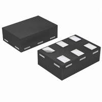
IP4221CZ6-S,115 NXP Semiconductors, IP4221CZ6-S,115 Datasheet - Page 9

IP4221CZ6-S,115
Manufacturer Part Number
IP4221CZ6-S,115
Description
IC USB2.0 DL ESD PROTECT 6-XSON
Manufacturer
NXP Semiconductors
Datasheet
1.IP4221CZ6-XS132.pdf
(13 pages)
Specifications of IP4221CZ6-S,115
Package / Case
6-XSON (Micropak™), SOT-886
Applications
USB
Number Of Circuits
4
Voltage - Working
3V
Technology
Diode Array
Channels
4 Channels
Breakdown Voltage
9 V
Capacitance
20 pF
Termination Style
SMD/SMT
Operating Temperature Range
- 40 C to + 85 C
Lead Free Status / RoHS Status
Lead free / RoHS Compliant
Power (watts)
-
Voltage - Clamping
-
Lead Free Status / Rohs Status
Lead free / RoHS Compliant
Other names
934061324115
NXP Semiconductors
9. Soldering of SMD packages
IP4221CZ6-S_1
Product data sheet
9.1 Introduction to soldering
9.2 Wave and reflow soldering
9.3 Wave soldering
This text provides a very brief insight into a complex technology. A more in-depth account
of soldering ICs can be found in Application Note AN10365 “Surface mount reflow
soldering description” .
Soldering is one of the most common methods through which packages are attached to
Printed Circuit Boards (PCBs), to form electrical circuits. The soldered joint provides both
the mechanical and the electrical connection. There is no single soldering method that is
ideal for all IC packages. Wave soldering is often preferred when through-hole and
Surface Mount Devices (SMDs) are mixed on one printed wiring board; however, it is not
suitable for fine pitch SMDs. Reflow soldering is ideal for the small pitches and high
densities that come with increased miniaturization.
Wave soldering is a joining technology in which the joints are made by solder coming from
a standing wave of liquid solder. The wave soldering process is suitable for the following:
Not all SMDs can be wave soldered. Packages with solder balls, and some leadless
packages which have solder lands underneath the body, cannot be wave soldered. Also,
leaded SMDs with leads having a pitch smaller than ~0.6 mm cannot be wave soldered,
due to an increased probability of bridging.
The reflow soldering process involves applying solder paste to a board, followed by
component placement and exposure to a temperature profile. Leaded packages,
packages with solder balls, and leadless packages are all reflow solderable.
Key characteristics in both wave and reflow soldering are:
Key characteristics in wave soldering are:
•
•
•
•
•
•
•
•
•
•
Through-hole components
Leaded or leadless SMDs, which are glued to the surface of the printed circuit board
Board specifications, including the board finish, solder masks and vias
Package footprints, including solder thieves and orientation
The moisture sensitivity level of the packages
Package placement
Inspection and repair
Lead-free soldering versus SnPb soldering
Process issues, such as application of adhesive and flux, clinching of leads, board
transport, the solder wave parameters, and the time during which components are
exposed to the wave
Solder bath specifications, including temperature and impurities
Rev. 01 — 29 April 2008
Dual USB 2.0 integrated quad with ESD protection (Pb-free)
IP4221CZ6-S
© NXP B.V. 2008. All rights reserved.
9 of 13


