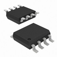
FDS8958A_F085 Fairchild Semiconductor, FDS8958A_F085 Datasheet - Page 3

FDS8958A_F085
Manufacturer Part Number
FDS8958A_F085
Description
MOSFET N/P-CH 30V DUAL 8-SOIC
Manufacturer
Fairchild Semiconductor
Series
PowerTrench®r
Datasheet
1.FDS8958A_F085.pdf
(8 pages)
Specifications of FDS8958A_F085
Fet Type
N and P-Channel
Fet Feature
Logic Level Gate
Rds On (max) @ Id, Vgs
28 mOhm @ 7A, 10V
Drain To Source Voltage (vdss)
30V
Current - Continuous Drain (id) @ 25° C
7A, 5A
Vgs(th) (max) @ Id
3V @ 250µA
Gate Charge (qg) @ Vgs
16nC @ 10V
Input Capacitance (ciss) @ Vds
575pF @ 15V
Power - Max
900mW
Mounting Type
Surface Mount
Package / Case
*
Configuration
Dual
Transistor Polarity
N and P-Channel
Resistance Drain-source Rds (on)
19 mOhms, 42 mOhms
Forward Transconductance Gfs (max / Min)
25 S, 10 S
Drain-source Breakdown Voltage
30 V
Gate-source Breakdown Voltage
20 V
Continuous Drain Current
7 A, - 5 A
Power Dissipation
2 W
Maximum Operating Temperature
+ 150 C
Mounting Style
SMD/SMT
Lead Free Status / RoHS Status
Lead free / RoHS Compliant
Other names
FDS8958A_F085TR
Available stocks
Company
Part Number
Manufacturer
Quantity
Price
Part Number:
FDS8958A_F085FDS8958A-F085
Manufacturer:
ON/ه®‰و£®ç¾ژ
Quantity:
20 000
FDS8958A_F085 Rev. A
Notes:
1. R
Scale 1 : 1 on letter size paper
2. Pulse Test: Pulse Width < 300µs, Duty Cycle < 2.0%
3. Starting TJ = 25°C, L = 3mH, I
Symbol
Switching Characteristics
t
t
t
t
Q
Q
Q
I
I
V
t
Q
Starting TJ = 25°C, L = 3mH, I
the drain pins. R
Electrical Characteristics
Drain–Source Diode Characteristics and Maximum Ratings
d(on)
r
d(off)
f
S
S M
rr
θJA
SD
g
gs
gd
rr
is the sum of the junction-to-case and case-to-ambient thermal resistance where the case thermal reference is defined as the solder mounting surface of
Turn-On Delay Time
Turn-On Rise Time
Turn-Off Delay Time
Turn-Off Fall Time
Total Gate Charge
Gate-Source Charge
Gate-Drain Charge
Maximum Continuous Drain-Source Diode Forward Current
Drain-Source Diode Forward
Voltage
Diode Reverse Recovery
Time
Diode Reverse Recovery
Charge
Maximum Plused Drain-Source Diode Forward Current
θJC
is guaranteed by design while R
a) 78°/W when
Parameter
mounted on a
0.5 in
copper
AS
AS
= 3A, V
= 6A, V
2
pad of 2 oz
DD
DD
= 30V, V
= 30V, V
(Note 2)
GS
GS
θCA
= 10V (Q2).
= 10V (Q1).
Q1
V
V
Q2
V
V
Q1
V
Q2
V
V
V
Q1
I
Q2
I
F
F
is determined by the user' s board design.
(continued)
DD
GS
DD
GS
DS
DS
GS
GS
= 7 A, d
= -5 A, d
= 15 V, I
= 10V, R
= -15 V, I
= -10V, R
= 15 V, I
= -15 V, I
= 0 V, I
= 0 V, I
Test Conditions
b) 125°/W when
iF
iF
S
S
/d
/d
D
D
mounted on a .02 in
pad of 2 oz copper
GEN
= 1.3 A
= -1.3 A
D
D
t
GEN
t
= 1 A,
= 7 A, V
= 100 A/µs
= 100 A/µs
= -5 A,V
= -1 A,
= 6 Ω
= 6 Ω
3
T
A
= 25°C unless otherwise noted
GS
GS
= 10 V
= -10 V
2
(Note 2)
(Note 2)
(Note 2)
Type Min
Q1
Q2
Q1
Q2
Q1
Q2
Q1
Q2
Q1
Q2
Q1
Q2
Q1
Q2
Q1
Q2
Q2
Q1
Q2
Q1
Q2
Q1
Q2
Q1
c) 135°/W when mounted on a
minimum pad.
-0.88
Typ Max Units
11.4
0.75
9.6
1.7
2.2
2.1
1.7
13
23
14
19
19
8
7
5
3
9
9
6
www.fairchildsemi.com
-1.3
-20
-1.2
1.3
1.2
16
13
16
14
10
24
37
25
17
20
6
nC
nC
nC
nS
nC
ns
ns
ns
ns
A
V
A


