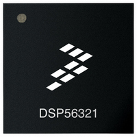
DSP56321VL200 Freescale Semiconductor, DSP56321VL200 Datasheet - Page 25

DSP56321VL200
Manufacturer Part Number
DSP56321VL200
Description
IC DSP 24BIT 200MHZ 196-MAPBGA
Manufacturer
Freescale Semiconductor
Series
DSP563xxr
Type
Fixed Pointr
Datasheet
1.DSP56321VL200R2.pdf
(84 pages)
Specifications of DSP56321VL200
Interface
Host Interface, SSI, SCI
Clock Rate
200MHz
Non-volatile Memory
ROM (576 B)
On-chip Ram
576kB
Voltage - I/o
3.30V
Voltage - Core
1.60V
Operating Temperature
-40°C ~ 100°C
Mounting Type
*
Package / Case
196-MAPBGA
Lead Free Status / RoHS Status
Lead free / RoHS Compliant
Available stocks
Company
Part Number
Manufacturer
Quantity
Price
Company:
Part Number:
DSP56321VL200
Manufacturer:
Freescale Semiconductor
Quantity:
10 000
Company:
Part Number:
DSP56321VL200R2
Manufacturer:
Freescale Semiconductor
Quantity:
10 000
Note: If an externally-supplied square wave voltage source is used, disable the internal oscillator circuit after
2.4.3
Freescale Semiconductor
Predivision factor
Predivider output clock frequency range
Total multiplication factor
Multiplication factor integer part
Multiplication factor numerator
Multiplication factor denominator
Double clock frequency range
Phase lock-in time
Notes:
No.
4
7
EXTAL cycle time
•
•
Instruction cycle time =
I
•
•
CYC
boot-up by setting XTLD (PCTL Register bit 2 = 1—see the DSP56321 Reference Manual). The external
square wave source connects to
Characteristics
With DPLL disabled
With DPLL enabled
With DPLL disabled
With DPLL enabled
1.
2.
3.
4.
Characteristics
Characteristics
= ET
Clock Generator (CLKGEN) and Digital PLL (DPLL)
EXTAL
The rise and fall time of this external clock should be 2 ns maximum.
Refer to Table 2-6 for a description of PDF and PDFR.
Measured at 50 percent of the input transition.
The indicated duty cycle is for the specified maximum frequency for which a part is rated. The minimum clock high or low time
required for correction operation, however, remains the same at lower operating frequencies; therefore, when a lower clock
frequency is used, the signal symmetry may vary from the specified duty cycle as long as the minimum high time and low time
requirements are met.
C
4
V
3
2
ILX
3
ET
H
Symbol
Table 2-5.
2
Table 2-6.
ET
I
CYC
Symbol
DDFR
PDFR
PDF
DPLT
MFI
MFN
MFD
C
MF
Figure 2-2.
4
1
1
ET
EXTAL and XTAL
DSP56321 Technical Data, Rev. 11
L
5.0 ns
5.0 ns
5.0 ns
10 ns
Min
Min
6.8
160
16
External Clock Operation (Continued)
1
5
5
0
1
200 MHz
3
ET
CLKGEN and DPLL Characteristics
5
200 MHz
C
External Input Clock Timing
62.5 ns
Max
150
1.6 µs
127
128
400
Max
16
32
15
15
∞
∞
6
is not used. Figure 2-2 shows the
Note:
Min
6.8
160
4.55 ns
4.55 ns
9.09 ns
4.55 ns
16
1
5
5
0
1
220 MHz
Min
5
220 MHz
The midpoint is 0.5 (V
Max
150
127
128
440
16
32
15
15
Midpoint
62.5 ns
1.6 µs
Max
6
∞
∞
Min
6.8
160
16
1
5
5
0
1
240 MHz
4.17 ns
4.17 ns
8.33 ns
4.17 ns
5
Min
240 MHz
Max
150
127
128
480
IHX
16
32
15
15
AC Electrical Characteristics
6
+ V
62.5 ns
V
1.6 µs
Max
IHX
ILX
∞
∞
EXTAL
Min
).
6.8
160
16
1
5
5
0
1
275 MHz
5
3.64 ns
3.64 ns
7.28 ns
3.64 ns
input signal.
Min
Max
150
127
128
550
275 MHz
16
32
15
15
6
62.5 ns
1.6 µs
Max
Unit
MHz
MHz
∞
∞
—
—
—
—
—
µs
2-5


