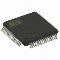
AT89C51CC03C-RDTIM Atmel, AT89C51CC03C-RDTIM Datasheet - Page 3

AT89C51CC03C-RDTIM
Manufacturer Part Number
AT89C51CC03C-RDTIM
Description
IC 8051 MCU FLASH 64K 64VQFP
Manufacturer
Atmel
Series
AT89C CANr
Datasheets
1.AT89C51CC03C-S3RIM.pdf
(198 pages)
2.AT89C51CC03C-S3RIM.pdf
(32 pages)
3.AT89C51CC03C-S3RIM.pdf
(27 pages)
4.AT89C51CC03C-S3RIM.pdf
(184 pages)
Specifications of AT89C51CC03C-RDTIM
Core Processor
8051
Core Size
8-Bit
Speed
40MHz
Connectivity
CAN, SPI, UART/USART
Peripherals
POR, PWM, WDT
Number Of I /o
36
Program Memory Size
64KB (64K x 8)
Program Memory Type
FLASH
Eeprom Size
2K x 8
Ram Size
2.25K x 8
Voltage - Supply (vcc/vdd)
3 V ~ 5.5 V
Data Converters
A/D 8x10b
Oscillator Type
External
Operating Temperature
-40°C ~ 85°C
Package / Case
64-TQFP, 64-VQFP
Lead Free Status / RoHS Status
Contains lead / RoHS non-compliant
Other names
AT89C51CC03CRDTIM
ISP Communication
Management
User Call Management Several Application Program Interface (API) calls are available to the application program to
Flash Memory
Management
Bootloader Configuration
Configuration and
Manufacturer
Information
Mapping and Default
Value of Hardware
Security Byte
4266C–CAN–03/08
The purpose of this process is to manage the communication and its protocol between the on-
chip bootloader and an external device (host). The on-chip bootloader implements a Serial pro-
tocol (see Section “Protocol”). This process translates serial communication frames (UART) into
Flash memory accesses (read, write, erase...).
selectively erase and program Flash pages. All calls are made through a common interface (API
calls) included in the bootloader. The purpose of this process is to translate the application
request into internal Flash Memory operations.
This process manages low level accesses to the Flash memory (performs read and write
accesses).
The table below lists Configuration and Manufacturer byte information used by the bootloader.
This information can be accessed through a set of API or ISP commands.
The 4 MSB of the Hardware Byte can be read/written by software (this area is called Fuse bits).
The 4 LSB can only be read by software and written by hardware in parallel mode (with parallel
programmer devices).
Note:
Mnemonic
BSB
SBV
SSB
EB
Manufacturer
Id1: Family code
Id2: Product Name
Id3: Product Revision
Bit Position
U: Unprogram = 1
P: Program = 0
7
6
5
4
3
2
1
0
X2B
BLJB
reserved
reserved
reserved
LB2
LB1
LB0
Mnemonic
Description
Boot Status Byte
Software Boot Vector
Software Security Byte
Extra Byte
Default Value
AT89C51CC03 UART Bootloader
U
U
U
U
U
U
P
P
Description
To start in x1 mode
To map the boot area in code area between F800h-
FFFFh
To lock the chip (see datasheet)
Default value
FFh
FCh
FFh
FFh
D7h
FFh
FEh
58h
3


