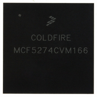
MCF5274CVM166 Freescale Semiconductor, MCF5274CVM166 Datasheet - Page 11

MCF5274CVM166
Manufacturer Part Number
MCF5274CVM166
Description
IC MPU 32BIT 166MHZ 256-MAPBGA
Manufacturer
Freescale Semiconductor
Series
MCF527xr
Datasheet
1.MCF5274LVM166J.pdf
(44 pages)
Specifications of MCF5274CVM166
Core Processor
Coldfire V2
Core Size
32-Bit
Speed
166MHz
Connectivity
EBI/EMI, Ethernet, I²C, SPI, UART/USART, USB
Peripherals
DMA, WDT
Number Of I /o
69
Program Memory Type
ROMless
Ram Size
64K x 8
Voltage - Supply (vcc/vdd)
1.4 V ~ 1.6 V
Oscillator Type
External
Operating Temperature
-40°C ~ 85°C
Package / Case
256-MAPBGA
Embedded Interface Type
I2C, SPI, USB, UART
Digital Ic Case Style
BGA
No. Of Pins
256
Operating Temperature Range
-40°C To +85°C
Processor Type
68K/ColdFire V2
Rohs Compliant
Yes
Family Name
MCF5xxx
Device Core
ColdFire
Device Core Size
32b
Frequency (max)
166MHz
Instruction Set Architecture
RISC
Operating Supply Voltage (max)
1.6V
Operating Supply Voltage (min)
1.4V
Operating Temp Range
-40C to 85C
Operating Temperature Classification
Industrial
Mounting
Surface Mount
Pin Count
256
Package Type
MA-BGA
Lead Free Status / RoHS Status
Lead free / RoHS Compliant
Eeprom Size
-
Program Memory Size
-
Data Converters
-
Lead Free Status / Rohs Status
Compliant
Available stocks
Company
Part Number
Manufacturer
Quantity
Price
Company:
Part Number:
MCF5274CVM166
Manufacturer:
Freescale Semiconductor
Quantity:
10 000
5.2.1.2
If V
impedance state. There is no limit on how long after V
must power down. V
power down or undesired high current will be in the ESD protection diodes. There are no requirements for
the fall times of the power supplies.
The recommended power down sequence is as follows:
5.3
5.4
5.5
5.6
Freescale Semiconductor
1. Drop V
2. Drop OV
•
•
•
•
•
•
•
•
•
•
•
•
DD
Place the decoupling capacitors as close to the pins as possible, but they can be outside the footprint
of the package.
0.1 μF and 0.01 μF at each supply input
Use bus buffers on all data/address lines for all off-board accesses and for all on-board accesses
when excessive loading is expected. See electricals.
Use external pull-up resistors on unused inputs. See pin table.
Use a multi-layer board with a separate ground plane.
Place the crystal and all other associated components as close to the EXTAL and XTAL (oscillator
pins) as possible.
Do not run a high frequency trace around crystal circuit.
Ensure that the ground for the bypass capacitors is connected to a solid ground trace.
Tie the ground trace to the ground pin nearest EXTAL and XTAL. This prevents large loop currents
in the vicinity of the crystal.
Tie the ground pin to the most solid ground in the system.
Do not connect the trace that connects the oscillator and the ground plane to any other circuit
element. This tends to make the oscillator unstable.
Tie XTAL to ground when an external oscillator is clocking the device.
is powered down first, then sense circuits in the I/O pads cause all output drivers to be in a high
Decoupling
Buffering
Pull-up Recommendations
Clocking Recommendations
Power Down Sequence
DD
DD
to 0 V.
MCF5275 Integrated Microprocessor Family Hardware Specification, Rev. 4
/SDV
DD
should not lag OV
DD
/PLLV
DD
supplies.
DD
, SDV
DD
DD
, or PLLV
powers down before OV
DD
going low by more than 0.4 V during
DD
Design Recommendations
, SDV
DD
, or PLLV
DD
11


