NLAS4717FCT1G ON Semiconductor, NLAS4717FCT1G Datasheet

IC SWITCH DUAL SPDT 10FLIPCHIP

NLAS4717FCT1G

Manufacturer Part Number
NLAS4717FCT1G
Description
IC SWITCH DUAL SPDT 10FLIPCHIP
Manufacturer
ON Semiconductor
Datasheet

Specifications of NLAS4717FCT1G

Function
Switch
Circuit
2 x SPDT
On-state Resistance
2.1 Ohm
Voltage Supply Source
Single Supply
Voltage - Supply, Single/dual (±)
1.8 V ~ 5.5 V
Current - Supply
1µA
Operating Temperature
-40°C ~ 85°C
Mounting Type
Surface Mount
Package / Case
10-FlipChip, 10-Microbump
Lead Free Status / RoHS Status
Lead free / RoHS Compliant
Other names
NLAS4717FCT1G
NLAS4717FCT1GOSTR

Available stocks

Company
Part Number
Manufacturer
Quantity
Price
Part Number:
NLAS4717FCT1G
Manufacturer:
ON Semiconductor
Quantity:
456
Part Number:
NLAS4717FCT1G
Manufacturer:
ON/安森美
Quantity:
20 000
NLAS4717
4.5 W High Bandwidth, Dual
SPDT Analog Switch
sub-micron silicon gate CMOS technology. The device is a dual
independent Single Pole Double Throw (SPDT) switch featuring two
low R
switching, assuring the switches never short the driver.
Features
Typical Applications
Important Information
*OVT
© Semiconductor Components Industries, LLC, 2007
May, 2007 - Rev. 9
The NLAS4717 is an advanced CMOS analog switch fabricated in
The device also features guaranteed Break-Before-Make (BBM)
The NLAS4717 is available in two small size packages:
normal supply voltages, with no damage to the devices or to signal
integrity.
Low R
Matching Between the Switches ±0.5 W
Wide Low Voltage Range: 1.8 V to 5.5 V
High Bandwidth > 40 MHz
1.65 V to 5.5 V Operating Range
Low Threshold Voltages on Pins 4 and 8 (CTRL Pins)
Ultra-Low Charge Injection ≤ 6.0 pC
Low Standby Current – I
OVT* on Pins 4 and 8 (CTRL Logic Pins)
Pb-Free Packages are Available
Cell Phones
PDAs
MP3s
Digital Still Cameras
ESD Protection:
Latchup Max Rating: 200 mA (Per JEDEC EIA/JESD78)
Pin-to-Pin Compatible with MAX4717
Overvoltage Tolerance (OVT) specific pins to operate higher than
Micro10:
Flip-Chip-10:
DS(on)
DS(on)
HBM = 2000 V, MM = 200 V
of 4.5 W at 3.0 V.
: 4.5 W @ 3.0 V
3.0 x 5.0 mm
2.0 x 1.5 mm
CC
= 1.0 nA (Max) @ T
A
= 25°C
1
†For information on tape and reel specifications,
NLAS4717FCT1
NLAS4717FCT1G Flip-Chip-10
NLAS4717MR2
NLAS4717MR2G
including part orientation and tape sizes, please
refer to our Tape and Reel Packaging Specifications
Brochure, BRD8011/D.
FLIP-CHIP-10
CASE 489AA
CASE 846B
Device
Micro10
IN_
0
1
A1
A
Y
W, WW = Work Week
G
ORDERING INFORMATION
http://onsemi.com
FUNCTION TABLE
= Assembly Location
= Year
= Pb-Free Package
Flip-Chip-10
(Pb-Free)
(Pb-Free)
Package
Micro10
Micro10
NO_
OFF
ON
Publication Order Number:
A1
DIAGRAMS
10
MARKING
1
AYWW G
NLAS4717/D
Tape & Reel
Tape & Reel
Tape & Reel
Tape & Reel
AYW G
4717
4717
Shipping
G
G
3000 /
3000 /
4000 /
4000 /
NC_
OFF
ON

Related parts for NLAS4717FCT1G

NLAS4717FCT1G Summary of contents

Page 1

... Work Week G IN_ 0 1 ORDERING INFORMATION Device NLAS4717FCT1 NLAS4717FCT1G Flip-Chip-10 NLAS4717MR2 NLAS4717MR2G †For information on tape and reel specifications, including part orientation and tape sizes, please refer to our Tape and Reel Packaging Specifications Brochure, BRD8011/D. 1 http://onsemi.com MARKING DIAGRAMS 4717 ...

Page 2

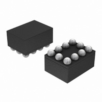
VCC 1 NO1 2 COM1 3 IN1 4 NC1 5 Micro10 (Top View) Figure 1. Device Circuit Diagrams and Pin Configurations MAXIMUM RATINGS Symbol V+ Positive DC Supply Voltage V Analog Input Voltage ( Digital ...

Page 3

ANALOG SWITCH CHARACTERISTICS - Digital Section Symbol Parameter R ON Resistance ON (Note Resistance ON Match Between Channels (Note 2 and Resistance FLAT[ON] Flatness (Note 4) I NO_, NC_ NO_[OFF] I Off-Leakage Current NC_[OFF] ...

Page 4

ANALOG SWITCH APPLICATION CHARACTERISTICS Symbol Parameter Q Charge Injection VISO Off-Isolation VCT Cross-T alk BW On-Channel -3.0 db Bandwidth THD Total Harmonic Distortion C NO_, NC_ NO_[OFF] C OFF-Capacitance NC_[OFF] C NO_, NC_ NO_[ON] C ON-Capacitance NC_[ON] NLAS4717 Condition V ...

Page 5

V (V) COM Figure 2. Low DS(on) 1.5 1.4 1.3 1.2 1.1 1.0 5.0 V 0.9 0.8 -40C +25C TEMPERATURE (°C) Figure 4. Delta ...

Page 6

-20 -40 -60 -80 -100 OFF-Isolation -120 -140 0.001 0.01 0.1 1 (MHz) Figure 8. Frequency Response NLAS4717 5 0 Cross-T alk - 1 5.0 V ...

Page 7

DUT V Output CC 0 Switch Select Pin DUT V Output CC 0.1 mF Open Input DUT Output Open Input NLAS4717 V CC Input GND V OUT 35 pF Output GND Figure 10. t (Time Break-Before-Make) BBM ...

Page 8

W Generator Channel switch control/s test socket is normalized. Off isolation is measured across an off channel. On loss is the bandwidth switch. V ISO V = Off Channel Isolation = 20 Log ISO V = ...

Page 9

0. PIN ONE CORNER A1 0. 0.075 0. 0. NLAS4717 PACKAGE DIMENSIONS ...

Page 10

... SEATING H PLANE *For additional information on our Pb-Free strategy and soldering details, please download the ON Semiconductor Soldering and Mounting Techniques Reference Manual, SOLDERRM/D. ON Semiconductor and are registered trademarks of Semiconductor Components Industries, LLC (SCILLC). SCILLC reserves the right to make changes without further notice to any products herein ...

Related keywords