NLAS4717FCT1G ON Semiconductor, NLAS4717FCT1G Datasheet - Page 2
NLAS4717FCT1G
Manufacturer Part Number
NLAS4717FCT1G
Description
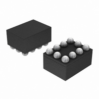
IC SWITCH DUAL SPDT 10FLIPCHIP
Manufacturer
ON Semiconductor
Datasheet
1.NLAS4717MR2G.pdf
(10 pages)
Specifications of NLAS4717FCT1G
Function
Switch
Circuit
2 x SPDT
On-state Resistance
2.1 Ohm
Voltage Supply Source
Single Supply
Voltage - Supply, Single/dual (±)
1.8 V ~ 5.5 V
Current - Supply
1µA
Operating Temperature
-40°C ~ 85°C
Mounting Type
Surface Mount
Package / Case
10-FlipChip, 10-Microbump
Lead Free Status / RoHS Status
Lead free / RoHS Compliant
Other names
NLAS4717FCT1G
NLAS4717FCT1GOSTR
NLAS4717FCT1GOSTR
Available stocks
Company
Part Number
Manufacturer
Quantity
Price
Company:

Part Number:
NLAS4717FCT1G
Manufacturer:
ON Semiconductor
Quantity:
456
Part Number:
NLAS4717FCT1G
Manufacturer:
ON/安森美
Quantity:
20 000


Stresses exceeding Maximum Ratings may damage the device. Maximum Ratings are stress ratings only. Functional operation above the
Recommended Operating Conditions is not implied. Extended exposure to stresses above the Recommended Operating Conditions may affect
device reliability.
1. Signal voltage on NC, NO, and COM exceeding VCC or GND are clamped by the internal diodes. Limit forward diode current to maximum
RECOMMENDED OPERATING CONDITIONS
MAXIMUM RATINGS
ANALOG SWITCH DC CHARACTERISTICS
Symbol
Symbol
Symbol
current rating.
V
V
t
V
I
V
V+
V+
V
I
T
r
V
I
PK
V
V
, t
IK
I
CC
IS
IN
IN
IS
A
IN
CC
IH
IL
IS
f
COM1
Positive DC Supply Voltage
Analog Input Voltage (V
Digital Select Input Voltage
DC Current, Into or Out of Any Pin (Continuous)
Peak Current (10% Duty Cycle)
DC Supply Voltage
Digital Select Input Voltage
Analog Input Voltage (NC, NO, COM)
Operating Temperature Range
Input Rise or Fall Time, SELECT
VCC
NO1
NC1
Input Logic High Voltage
IN1
Input Logic Low Voltage
Input Leakage Current
Power Supply Range
Analog Signal Range
Supply Current
Parameter
1
2
3
4
5
(Top View)
Figure 1. Device Circuit Diagrams and Pin Configurations
Micro10
NO
, V
NC
, or V
V
Parameter
Parameter
OUT
V
V
COM
IN
IN
Key parameter
V
I
I
OUT
OUT
I
10
Condition
= V
OUT
OUT
– V
9
8
7
6
) (Note 1)
= -V
CC
CC
≤ 20 mA
≤ 20 mA
All
COM2
IN2
NC2
GND
= 0 mA
http://onsemi.com
NO2
= 0.1 V
CC
or GND
or GND
NLAS4717
- 0.1 V
2
V
V
CC
CC
1.65 to 2.2
1.65 to 2.2
2.7 to 3.6
4.5 to 5.5
2.7 to 3.6
4.5 to 5.5
COM1
V
NO1
NC1
CC
= 3.3 V $ 0.3 V
= 5.0 V $ 0.5 V
5.0
1.8
3.3
5.0
IN1
-
-
(V)
C
C
C
C
1
2
3
4
V
Flip-Chip-10
V
CC
(Top View)
CC
-100
1.65
Min
2.0
GND
VCC
x 0.55
-
-
-
-
-
-
0
*0.5 v V
x 0.5
B
B
1
4
-40 °C to +85°C
GND
GND
*0.5 v V
Min
-40
1.8
0
0
*0.5 to )7.0
Value
$100
$200
IS
v V
A
A
A
A
I
1
2
3
4
v)7.0
V
V
CC
CC
CC
NC2
IN2
COM2
+100
NO2
Max
Max
V
V
+85
100
0.8
5.5
1.0
1.0
1.0
5.5
5.5
20
-
-
-
CC
CC
)0.5
x 0.2
x 0.2
ns/V
Unit
Unit
mA
mA
°C
Unit
V
V
V
V
V
V
nA
mA
V
V
V
V
Related parts for NLAS4717FCT1G
Image
Part Number
Description
Manufacturer
Datasheet
Request
R

Part Number:
Description:
Dual Spdt High Bandwidth Usb 2.0 Compliant Analog Switch
Manufacturer:
ON Semiconductor
Datasheet:
Part Number:
Description:
ON Semiconductor [VOLTAGE REGULATOR]
Manufacturer:
ON Semiconductor
Datasheet:
Part Number:
Description:
357-036-542-201 CARDEDGE 36POS DL .156 BLK LOPRO
Manufacturer:
ON Semiconductor
Datasheet:
Part Number:
Description:
357-036-542-201 CARDEDGE 36POS DL .156 BLK LOPRO
Manufacturer:
ON Semiconductor
Datasheet:
Part Number:
Description:
357-036-542-201 CARDEDGE 36POS DL .156 BLK LOPRO
Manufacturer:
ON Semiconductor
Datasheet:
Part Number:
Description:
357-036-542-201 CARDEDGE 36POS DL .156 BLK LOPRO
Manufacturer:
ON Semiconductor
Datasheet:
Part Number:
Description:
357-036-542-201 CARDEDGE 36POS DL .156 BLK LOPRO
Manufacturer:
ON Semiconductor
Datasheet:
Part Number:
Description:
357-036-542-201 CARDEDGE 36POS DL .156 BLK LOPRO
Manufacturer:
ON Semiconductor
Datasheet:
Part Number:
Description:
357-036-542-201 CARDEDGE 36POS DL .156 BLK LOPRO
Manufacturer:
ON Semiconductor
Datasheet:
Part Number:
Description:
357-036-542-201 CARDEDGE 36POS DL .156 BLK LOPRO
Manufacturer:
ON Semiconductor
Datasheet:
Part Number:
Description:
357-036-542-201 CARDEDGE 36POS DL .156 BLK LOPRO
Manufacturer:
ON Semiconductor
Datasheet:
Part Number:
Description:
357-036-542-201 CARDEDGE 36POS DL .156 BLK LOPRO
Manufacturer:
ON Semiconductor
Datasheet:
Part Number:
Description:
Manufacturer:
ON Semiconductor
Datasheet:
Part Number:
Description:
Manufacturer:
ON Semiconductor
Datasheet: