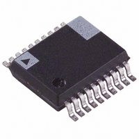
ADE7761AARS-RL Analog Devices Inc, ADE7761AARS-RL Datasheet - Page 4

ADE7761AARS-RL
Manufacturer Part Number
ADE7761AARS-RL
Description
IC DETECTOR ENERGY METER 20-SSOP
Manufacturer
Analog Devices Inc
Datasheet
1.ADE7761AARSZ-RL.pdf
(24 pages)
Specifications of ADE7761AARS-RL
Input Impedance
400 KOhm
Measurement Error
0.1%
Voltage - I/o High
2.4V
Voltage - I/o Low
0.8V
Current - Supply
3mA
Voltage - Supply
4.75 V ~ 5.25 V
Operating Temperature
-40°C ~ 85°C
Mounting Type
Surface Mount
Package / Case
20-SSOP (0.200", 5.30mm Width)
Meter Type
Single Phase
Lead Free Status / RoHS Status
Contains lead / RoHS non-compliant
ADE7761A
Parameter
LOGIC INPUTS
LOGIC OUTPUTS
POWER SUPPLY
1
2
3
4
5
TIMING CHARACTERISTICS
V
initial release and after any redesign or process change that might affect this parameter. See Figure 2.
Table 2.
Parameter
t
t
t
t
t
t
1
1
2
3
4
5
6
See plots in the Typical Performance Characteristics section.
See the Terminology section for explanation of specifications.
See the Fault Detection section for explanation of fault detection functionality.
See the Missing Neutral Detection section for explanation of missing neutral detection functionality.
Sample tested during initial release and after any redesign or process change that might affect this parameter.
The pulse widths of F1, F2, and CF are not fixed for higher output frequencies. See the Transfer Function section.
1
DD
1
PGA, SCF, S1, and S0
CF, REVP, and FAULT
F1 and F2
V
V
DD
DD
= 5 V ± 5%, AGND = DGND = 0 V, on-chip reference, on-chip oscillator, T
Input High Voltage, V
Input Low Voltage, V
Input Current, I
Input Capacitance, C
Output High Voltage, V
Output Low Voltage, V
Output High Voltage, V
Output Low Voltage, V
5
5
IN
Value
120
See Table 7
1/2 t
90
See Table 8
CLKIN/4
INL
IN
INH
2
OH
OH
OH
OH
F1
F2
CF
Unit
ms
s
s
ms
s
s
t
4
Value
2.4
0.8
±3
10
4
1
4
1
4.75
5.25
3
Figure 2. Timing Diagram for Frequency Outputs
t
1
Test Conditions/Comments
F1 and F2 Pulse Width (Logic High).
Output Pulse Period. See the Transfer Function section.
Time Between F1 Falling Edge and F2 Falling Edge.
CF Pulse Width (Logic High).
CF Pulse Period. See the Transfer Function section.
Minimum Time Between F1 and F2 Pulse.
Unit
V, min
V, max
μA, max
pF, max
V, min
V, max
V, min
V, max
V, min
V, max
mA, max
t
3
t
5
t
6
t
2
Rev. 0 | Page 4 of 24
Test Conditions/Comments
V
V
Typical 10 nA, V
V
V
V
V
For specified performance
5 V − 5%
5 V + 5%
DD
DD
DD
DD
DD
DD
= 5 V ± 5%
= 5 V ± 5%
= 5 V ± 5%
= 5 V ± 5%
= 5 V ± 5%, I
= 5 V ± 5%, I
MIN
to T
MAX
IN
= −40°C to +85°C. Sample tested during
SOURCE
SINK
= 0 V to V
= 10 mA
= 10 mA
DD


