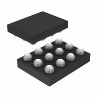
LM3530UME-25A/NOPB National Semiconductor, LM3530UME-25A/NOPB Datasheet - Page 26

LM3530UME-25A/NOPB
Manufacturer Part Number
LM3530UME-25A/NOPB
Description
IC LED DRVR PRGRAM I2C 10LED SMD
Manufacturer
National Semiconductor
Series
PowerWise®r
Datasheet
1.LM3530UME-40NOPB.pdf
(44 pages)
Specifications of LM3530UME-25A/NOPB
Topology
PWM, Step-Up (Boost)
Number Of Outputs
1
Internal Driver
Yes
Type - Primary
Backlight
Type - Secondary
White LED
Frequency
500kHz
Voltage - Supply
2.7 V ~ 5.5 V
Mounting Type
Surface Mount
Package / Case
12-XFBGA
Operating Temperature
-40°C ~ 85°C
Current - Output / Channel
Adjustable
Lead Free Status / RoHS Status
Lead free / RoHS Compliant
Voltage - Output
-
Other names
LM3530UME-25A/NOPBTR
www.national.com
I
START AND STOP CONDITION
The LM3530 is controlled via an I
START and STOP conditions classify the beginning and the
end of the I
transitioning from HIGH to LOW while SCL is HIGH. A STOP
condition is defined as SDA transitioning from LOW to HIGH
while SCL is HIGH. The I
I
The 7bit chip address for the LM3530 is (0x38, or 0x39) for
the 40V version and (0x36) for the 25V version. After the
START condition, the I
followed by an eighth bit (LSB) read or write (R/W). R/W= 0
TRANSFERRING DATA
Every byte on the SDA line must be eight bits long, with the
most significant bit (MSB) transferred first. Each byte of data
must be followed by an acknowledge bit (ACK). The acknowl-
edge related clock pulse (9th clock pulse) is generated by the
master. The master then releases SDA (HIGH) during the 9th
2
2
C-COMPATIBLE ADDRESS
C-Compatible Interface
2
C session. A START condition is defined as SDA
2
C master sends the 7-bit chip address
2
C master always generates the
2
C-compatible interface.
FIGURE 16. I
FIGURE 17. I
FIGURE 15. Start and Stop Sequences
2
2
C-Compatible Chip Address (0x38)
C-Compatible Chip Address (0x36)
26
START and STOP conditions. The I
after a START condition and free after a STOP condition.
During data transmission, the I
peated START conditions. A START and a repeated START
conditions are equivalent function-wise. The data on SDA
must be stable during the HIGH period of the clock signal
(SCL). In other words, the state of SDA can only be changed
when SCL is LOW.
indicates a WRITE and R/W = 1 indicates a READ. The sec-
ond byte following the chip address selects the register ad-
dress to which the data will be written. The third byte contains
the data for the selected register.
clock pulse. The LM3530 pulls down SDA during the 9th clock
pulse, signifying an acknowledge. An acknowledge is gener-
ated after each byte has been received.
There are fourteen 8-bit registers within the LM3530 as de-
tailed in
Table
4.
2
C master can generate re-
2
30086637
C bus is considered busy
30086638
30086639


