UPC2756TB-EVAL CEL, UPC2756TB-EVAL Datasheet - Page 6
UPC2756TB-EVAL
Manufacturer Part Number
UPC2756TB-EVAL
Description
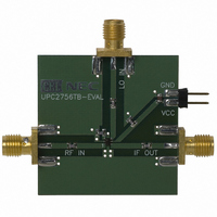
EVAL BOARD FOR UPC2756TB
Manufacturer
CEL
Type
Downconverterr
Specifications of UPC2756TB-EVAL
Contents
Board
Product
RFID Readers
Dimensions
50 mm x 50 mm x 1.6 mm
For Use With/related Products
UPC2756TB
Lead Free Status / RoHS Status
Contains lead / RoHS non-compliant
Lead Free Status / RoHS Status
Contains lead / RoHS non-compliant, Lead free / RoHS Compliant


PIN EXPLANATION
APPLICATION
does not have 50 Ω input/output impedance, but electrical characteristics such as conversion gain and
intermodulation distortion are described herein on these conditions without impedance matching. So, you should
understand that conversion gain and intermodulation distortion at input level will vary when you improve VS of RF
input with external circuit (50 Ω termination or impedance matching).
External circuits of the IC are explained in a following application note.
• To RF and IF port : Application Note “Usage and Application Characteristics of µ µ µ µ PC2757T, µ µ µ µ PC2758T and
4
Pin
No.
1
2
3
4
5
6
Note Pin voltage is measured at V
This IC is guaranteed on the test circuit constructed with 50 Ω equipment and transmission line. This IC, however,
µ µ µ µ PC8112T, 3-V Power Supply, 1.9-GHz Frequency Down Converter ICs for Cellular/Cordless Telephone and
Portable Wireless Communication” (P11997E)
Pin Name
IFoutput
RFinput
GND
LO
LO
V
CC
1
2
2.7 to 3.3
Applied
Voltage
(V)
–
0
–
–
–
Voltage
(V)
Pin
1.2
1.2
1.2
1.7
–
–
Note
CC
This pin is RF input for mixer designed as double
balance type.
This circuit contributes to suppress spurious signal
with minimum LO and bias power consumption.
Also this symmetrical circuit can keep specified
performance insensitive to process-condition
distribution.
This pin must be externally coupled to front stage
with capacitor for DC cut.
Must be connected to the system ground with
minimum inductance. Ground pattern on the board
should be formed as wide as possible.
(Track length should be kept as short as possible.)
These pins are both base-collector of oscillator. This
oscillator is designed as differential amplifier type.
3 pin and 4 pin should be externally equipped with
tank resonator circuit in order to oscillate with
feedback loop. Also this symmetrical circuit can keep
specified performance insensitive to process-
condition distribution.
Each pin must be externally coupled to tank circuit
with capacitor for DC cut.
Supply voltage 3.0 ± 0.3 V for operation. Must be
connected bypass capacitor (e.g. 1 000 pF) to
minimize ground impedance.
This pin is output from IF buffer amplifier designed as
single-ended push-pull type.
This pin is assigned for emitter follower output with
low-impedance. This pin must be externally coupled
to next stage with capacitor for DC cut.
= 3.0 V
Data Sheet P12807EJ3V0DS
Function and Application
3
Equivalent Circuit
V
µ µ µ µ PC2756TB
V
CC
CC
6
4
V
1
CC
Related parts for UPC2756TB-EVAL
Image
Part Number
Description
Manufacturer
Datasheet
Request
R

Part Number:
Description:
IC MMIC DWN-CNVRTR SOT-363
Manufacturer:
CEL
Datasheet:
Part Number:
Description:
MMIC DOWN CONV 3V 2GHZ SOT-26
Manufacturer:
CEL
Datasheet:
Part Number:
Description:
MMIC DOWN CONV 3V 2GHZ SOT-26
Manufacturer:
CEL
Datasheet:
Part Number:
Description:
MMIC DOWN CONV 3V 2GHZ SOT-26
Manufacturer:
CEL
Datasheet:

Part Number:
Description:
Dantona CEL-V325-HC Cell Phone Battery Fits Motorola Q & BT-50
Manufacturer:
DANTONA INDUSTRIES
Part Number:
Description:
FRS RADIO BATTERIES 3.6 VOLTS / 1600 MAH
Manufacturer:
DANTONA INDUSTRIES
Part Number:
Description:
LITHIUM ION 900MA FOR USE WITH NOKIA 3360 CELL PHONE
Manufacturer:
DANTONA INDUSTRIES
Part Number:
Description:
CELL PHONE BATTERY FOR MOTOROLA V3 CELLULAR PHONE
Manufacturer:
DANTONA INDUSTRIES
Part Number:
Description:
Transistor Output Optocouplers DISC BY CEL 6/00 SO-6 PHOTOCOUPLER
Manufacturer:
CEL
Datasheet:
Part Number:
Description:
Transistor Output Optocouplers DISC BY CEL 8/00 DIP-6 PHOTO COUPLER
Manufacturer:
CEL
Datasheet:
Part Number:
Description:
Transistor Output Optocouplers DISC BY CEL 11/00 DIP-6 PHOTO COUPLER
Manufacturer:
CEL
Datasheet:
Part Number:
Description:
Transistor Output Optocouplers DISC BY CEL 6/00 DIP-6 PHOTO COUPLER
Manufacturer:
CEL
Datasheet:
Part Number:
Description:
Transistor Output Optocouplers DISC BY CEL 5/00 DIP-6 PHOTO COUPLER
Manufacturer:
CEL
Datasheet: