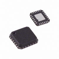
ADL5330ACPZ-REEL7 Analog Devices Inc, ADL5330ACPZ-REEL7 Datasheet - Page 15

ADL5330ACPZ-REEL7
Manufacturer Part Number
ADL5330ACPZ-REEL7
Description
IC AMP/ATTENUATOR RF VAR 24LFCSP
Manufacturer
Analog Devices Inc
Datasheet
1.ADL5330ACPZ-REEL7.pdf
(24 pages)
Specifications of ADL5330ACPZ-REEL7
Design Resources
Stable, Closed-Loop Automatic Power Control for RF Appls (CN0050)
Current - Supply
250mA
Frequency
10MHz ~ 3GHz
Gain
10dB
P1db
1.2dBm
Package / Case
24-VFQFN, 24-CSP Exposed Pad
Rf Type
Cellular, CDMA2000, W-CDMA, GSM
Test Frequency
2.7GHz
Voltage - Supply
4.75 V ~ 5.25 V
No. Of Amplifiers
1
No. Of Channels
1
Supply Voltage Range
4.75V To 5.25V
Amplifier Case Style
LFCSP
No. Of Pins
24
Operating Temperature Range
-40°C To +85°C
Termination Type
SMD
Lead Free Status / RoHS Status
Lead free / RoHS Compliant
Noise Figure
-
Lead Free Status / RoHS Status
Lead free / RoHS Compliant, Lead free / RoHS Compliant
Other names
ADL5330ACPZ-REEL7
ADL5330ACPZ-REEL7TR
ADL5330ACPZ-REEL7TR
Available stocks
Company
Part Number
Manufacturer
Quantity
Price
Company:
Part Number:
ADL5330ACPZ-REEL7
Manufacturer:
VISHAY
Quantity:
1 600
Part Number:
ADL5330ACPZ-REEL7
Manufacturer:
ADI/亚德诺
Quantity:
20 000
GAIN CONTROL INPUT
When the VGA is enabled, the voltage applied to the GAIN pin
sets the gain. The input impedance of the GAIN pin is 1 MΩ.
The gain control voltage range is between 0 V and +1.4 V, which
corresponds to a typical gain range between −38 dB and
+22 dB. The useful lower limit of the gain control voltage
increases at high frequencies to about 0.5 V and 0.6 V for
2.2 GHz and 2.7 GHz, respectively. The supply current to the
ADL5330 can vary from approximately 100 mA at low gain
control voltages to 215 mA at 1.4 V.
The 1 dB input compression point remains constant at 3 dBm
through the majority of the gain control range, as shown in
Figure 9 through Figure 13. The output compression point
increases dB for dB with increasing gain setting. The noise floor
is constant up to 1 V where it begins to rise.
The bandwidth on the gain control pin is approximately 3 MHz.
Figure 14 shows the response time of a pulse on the GAIN pin.
AUTOMATIC GAIN CONTROL
Although the ADL5330 provides accurate gain control, precise
regulation of output power can be achieved with an automatic
gain control (AGC) loop. Figure 36 shows the ADL5330 in an
AGC loop. The addition of the log amp (AD8318/AD8315) or a
TruPwr™ detector (AD8362) allows the AGC to have improved
temperature stability over a wide output power control range.
To operate the ADL5330 in an AGC loop, a sample of the
output RF must be fed back to the detector (typically using a
directional coupler and additional attenuation). A setpoint
voltage is applied to the VSET input of the detector while
VOUT is connected to the GAIN pin of the ADL5330. Based on
the detector’s defined linear-in-dB relationship between VOUT
and the RF input signal, the detector adjusts the voltage on the
GAIN pin (the detector’s VOUT pin is an error amplifier
output) until the level at the RF input corresponds to the
applied setpoint voltage. The GAIN setting settles to a value
that results in the correct balance between the input signal level
at the detector and the setpoint voltage.
Rev. A | Page 15 of 24
The detector’s error amplifier uses C
capacitor pin, to integrate the error signal (in the form of a
current). A capacitor must be connected to C
bandwidth and to ensure loop stability.
The basic connections for operating the ADL5330 in an AGC
loop with the AD8318 are shown in Figure 37. The AD8318 is a
1 MHz to 8 GHz precision demodulating logarithmic amplifier.
It offers a large detection range of 60 dB with ±0.5 dB tempera-
ture stability. This configuration is similar to Figure 36.
The gain of the ADL5330 is controlled by the output pin of the
AD8318. This voltage, VOUT, has a range of 0 V to near VPOS.
To avoid overdrive recovery issues, the AD8318 output voltage
can be scaled down using a resistive divider to interface with the
0 V to 1.4 V gain control range of ADL5330.
A coupler/attenuation of 23 dB is used to match the desired
maximum output power from the VGA to the top end of the
linear operating range of the AD8318 (at approximately −5 dBm
at 900 MHz).
RFIN
DAC
INHI
INLO
VSET
VPOS
Figure 36. ADL5330 in AGC Loop
+5V
LOG AMP OR
DETECTOR
ADL5330
TRUPWR
VOUT
CLPF
GAIN
COMM
OPLO
OPHI
RFIN
FLT
+5V
, a ground-referenced
FLT
to set the loop
ADL5330
DIRECTIONAL
COUPLER
ATTENUATOR


