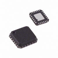
ADL5330ACPZ-REEL7 Analog Devices Inc, ADL5330ACPZ-REEL7 Datasheet - Page 22

ADL5330ACPZ-REEL7
Manufacturer Part Number
ADL5330ACPZ-REEL7
Description
IC AMP/ATTENUATOR RF VAR 24LFCSP
Manufacturer
Analog Devices Inc
Datasheet
1.ADL5330ACPZ-REEL7.pdf
(24 pages)
Specifications of ADL5330ACPZ-REEL7
Design Resources
Stable, Closed-Loop Automatic Power Control for RF Appls (CN0050)
Current - Supply
250mA
Frequency
10MHz ~ 3GHz
Gain
10dB
P1db
1.2dBm
Package / Case
24-VFQFN, 24-CSP Exposed Pad
Rf Type
Cellular, CDMA2000, W-CDMA, GSM
Test Frequency
2.7GHz
Voltage - Supply
4.75 V ~ 5.25 V
No. Of Amplifiers
1
No. Of Channels
1
Supply Voltage Range
4.75V To 5.25V
Amplifier Case Style
LFCSP
No. Of Pins
24
Operating Temperature Range
-40°C To +85°C
Termination Type
SMD
Lead Free Status / RoHS Status
Lead free / RoHS Compliant
Noise Figure
-
Lead Free Status / RoHS Status
Lead free / RoHS Compliant, Lead free / RoHS Compliant
Other names
ADL5330ACPZ-REEL7
ADL5330ACPZ-REEL7TR
ADL5330ACPZ-REEL7TR
Available stocks
Company
Part Number
Manufacturer
Quantity
Price
Company:
Part Number:
ADL5330ACPZ-REEL7
Manufacturer:
VISHAY
Quantity:
1 600
Part Number:
ADL5330ACPZ-REEL7
Manufacturer:
ADI/亚德诺
Quantity:
20 000
ADL5330
Table 5. Evaluation Board Configuration Options
Components
C1 to C4, C7 to C10, C13,
C14, R2, R4, R5, R6, R12
T1, C5, C6
T2, C11, C12, L1, L2
SW1, R1, R13
C15 to C18, M1 to M18
Function
Power Supply Decoupling. The nominal supply decoupling consists of
100 pF and 0.1 μF capacitors at each power supply pin (the VPS2 pins, Pin 18
to Pin 22, share a pair of decoupling capacitors because of their proximity). A
series inductor or small resistor can be placed between the capacitors for
additional decoupling.
Input Interface. The 1:1 balun transformer T1 converts a 50 Ω single-ended
input to the 50 Ω differential input. C5 and C6 are dc blocks.
Output Interface. The 1:1 balun transformer T2 converts the 50 Ω differential
output to 50 Ω single-ended output. C11 and C2 are dc blocks. L3 and
L4 provide dc biases for the output.
Enable Interface. The ADL5330 is enabled by applying a logic high voltage
to the ENBL pin by placing a jumper across SW1 to the O position. Remove
the jumper for disable. To exercise the enable function by applying an
external high or low voltage, use the pin labeled O on the SW1 header.
Alternate Input/Output Interface. The circuit side of the evaluation board
offers an alternate RF input and output interface. A lumped-element balun
can be built using L and C components instead of using the balun
transformer (see the Applications section). The components, M1 through
M9, are used for the input, and M10 through M18 are used for the output.
To use the alternate RF paths, disconnect the dc blocking capacitors
(Capacitor C5 and Capacitor C6 for the input and Capacitor C11 and
Capacitor C12 for the output). Place 100 pF dc blocking capacitors on
C15, C16, C17, and C18. Use the alternate set of SMA connectors,
INPUT2 and OUT2.
Rev. A | Page 22 of 24
Default Conditions
C1, C4, C7, C10, C13 = 100 pF
C2, C3, C8, C9, C14 = 0.1 μF
R2, R4, R5, R6, R12 = 0 Ω
T1 = ETC1-1-13 (M/A-COM)
C5, C6 = 100 pF (size 0603)
T2 = ETC1-1-13 (M/A-COM)
C11, C12 = 100 pF (size 0603)
L1, L2 = 120 nH (size 0805)
SW1 = installed
R1 = 0 Ω (size 0402)
R13 = 10 kΩ (size 0402)
M1 to M18 = not installed
C15 to C18 = not installed
(size 0603)
(size 0603)
(size 0402)
(size 0603)
(size 0603)


