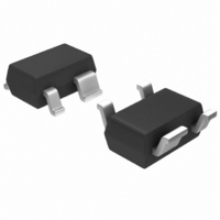
MGA-72543-BLKG Avago Technologies US Inc., MGA-72543-BLKG Datasheet - Page 16

MGA-72543-BLKG
Manufacturer Part Number
MGA-72543-BLKG
Description
IC AMP MMIC LNA GAAS 3V SOT-343
Manufacturer
Avago Technologies US Inc.
Type
General Purpose Amplifierr
Datasheet
1.MGA-72543-TR1G.pdf
(21 pages)
Specifications of MGA-72543-BLKG
Noise Figure
1.5dB ~ 1.8dB
Package / Case
SC-70-4, SC-82-4, SOT-323-4, SOT-343
Current - Supply
60mA ~ 70mA
Frequency
100MHz ~ 6GHz
Gain
13.5dB ~ 15.5dB
P1db
11.2dBm
Rf Type
CDMA, TDMA, W-CDMA
Test Frequency
2.4GHz
Voltage - Supply
2.7V ~ 3.3V
Mounting Style
SMD/SMT
Technology
Low Noise Amplifier
Number Of Channels
1
Operating Frequency
6000 MHz
Operating Supply Voltage
3 V
Supply Current
60 mA
Maximum Power Dissipation
250 mW
Maximum Operating Temperature
+ 150 C
Manufacturer's Type
Low Noise Amplifier
Frequency (max)
6GHz
Operating Supply Voltage (min)
2.7V
Operating Supply Voltage (typ)
3V
Operating Supply Voltage (max)
4.2V
Package Type
SOT-343
Mounting
Surface Mount
Pin Count
3 +Tab
Noise Figure (typ)
1.7@6000MHzdB
Lead Free Status / RoHS Status
Lead free / RoHS Compliant
Lead Free Status / RoHS Status
Lead free / RoHS Compliant, Lead free / RoHS Compliant
Other names
516-1953
MGA-72543-BLKG
MGA-72543-BLKG
Available stocks
Company
Part Number
Manufacturer
Quantity
Price
Part Number:
MGA-72543-BLKG
Manufacturer:
AVAGO/安华高
Quantity:
20 000
Controlling the Switch
The state of the MGA-72543 (amplifier or bypass mode)
is controlled by the device current. For device currents
greater than 5 mA, the MGA-72543 functions as an am-
plifier. If the device current is set to zero, the MGA- 72543
is switched into a bypass mode in which the amplifier is
turned off and the signal is routed around the amplifier
with a loss of approximately 2.5 dB.
The bypass state is normally engaged in the presence of
high input levels to prevent distortion of the signal that
might occur in the amplifier. In the bypass state, the input
TOI is very high, typically +39 dBm at 1900 MHz.
The simplest method of placing the MGA-72543 into the
bypass mode is to open-circuit the ground terminals at
Pins 1 and 4. With the ground connection open, the inter-
nal control circuit of the MGA-72543 auto-switches from
the amplifier mode into a bypass state and the device
current drops to near zero. Nominal current in the bypass
state is 2 μA with a maximum of 15 μA.
Figure 9. MGA-72543 Amplifier/Bypass State Switching.
An electronic switch can be used to control states as
shown in Figure 9. The control switch could be imple-
mented with either a discrete transistor or simple IC.
The speed at which the MGA-72543 switches between
states is extremely fast and will normally be limited by
the time constants of external circuit components, such
as the bias circuit and the bypass and blocking capacitors.
The input and output of the MGA-72543 while in the
bypass state are internally matched to 50 É∂. The input
return loss can be further improved at 1900 MHz by
adding a 2.7 to 3.9 nH series inductor added to the input.
This is the same approximate value of inductor that is
used to improve input match when the MGA-72543 is in
the amplifier state.
16
3
1
R
bias
4
2
Bypass Switch
Enable
Thermal Considerations
Good thermal design is always an important consider-
ation in the reliable use of any device, since the Mean
Time To Failure (MTTF) of semiconductors is inversely
proportional to the operating temperature.
The MGA-72543 is a comparatively low power dissipation
device and, as such, operates at conservative tempera-
tures. When biased at 3 volts and 20 mA for LNA applica-
tions, the power dissipation is 3.0 volts x 20 mA, or 60 mW.
The temperature increment from the RFIC channel to its
case is then 0.060 watt x 200°C/watt, or only 12°C. Sub-
tracting the channel-to-case temperature rise from the
suggested maximum junction temperature of 150°C, the
resulting maximum allowable case temperature is 138°C.
The worst case thermal situation occurs when the MGA-
72543 is operated at its Maximum Operating conditions in
an effort to maximize output power or achieve minimum
distortion. A similar calculation for the Maximum Operat-
ing bias of 4.2 volts and 60 mA yields a maximum allow-
able case temperature of 100°C. This calculation further
assumes the worst case of no RF power being extracted
from the device. When operated in a saturated mode,
both power-added efficiency and the maximum allowable
case temperature will increase.
Note: “Case” temperature for surface mount packages
such as the SOT-343 refers to the interface between the
package pins and the mounting surface, i.e., the tempera-
ture at the PCB mounting pads. The primary heat path
from the RFIC chip to the system heatsink is by means of
conduction through the package leads and ground vias
to the groundplane of the PCB.
PCB Layout and Grounding
When laying out a printed circuit board for the MGA-
72543, several points should be considered. Of primary
concern is the RF bypassing of the ground terminals when
the device is biased using the source resistor method.


