ATR7040-PVPG Atmel, ATR7040-PVPG Datasheet
ATR7040-PVPG
Specifications of ATR7040-PVPG
Available stocks


Related parts for ATR7040-PVPG


ATR7040-PVPG Summary of contents
Page 1
... Circuitry The PA, ATR7040, consists of a three-stage amplifier with a typical output power of 25 dBm. The output stage was implemented using an open-collector structure. Power up, power down, and output level are controlled at bias control pin 6 (V 5.8 GHz WDCT ...
Page 2
... Figure 1-1. Block Diagram VCC1 7 RFIN 10 13 VCTL ATR7040 2 VCC2 6 ATR7040 Matching Bias control PADDLE 14 GND GND RFOUT/VCC3 2 Matching RFOUT/VCC3 3 15 VCC_CTL 4868C–DECT–05/06 ...
Page 3
... Control voltage for power ramping 14 GND Ground 15 VCC_CTL Supply voltage for biasing control block 16 NC Not connected PADDLE – Ground Note: 1. Pin can be connected to paddle for increased GND area 4868C–DECT–05/ ATR7040 RFOUT/VCC3 RFOUT/VCC3 3 10 RFIN GND on the NC PADDLE (1) (1) (1) (1) (1) (1) (1) (1) ATR7040 3 ...
Page 4
... The part may not survive all maximums applied simultaneously. Electrostatic sensitive device. Observe precautions for handling. 4. Thermal Resistance Parameters Junction ambient package QFN16, 3 × 3, slug soldered on PCB 5. Operating Range Parameters Supply voltage Operating frequency range Ambient temperature range ATR7040 4 Symbol Value 400 cc T 150 ...
Page 5
... At saturated output power VCC C6 slug TRL1 VCTL VCC Symbol Min. Typ. 5100 V 2.7 3 sat P – 1.0 ctl V ctl I 90 ctl –7 ISO PAE 35 I 250 100 RFOUT TRL2 ATR7040 = 1 ms, on Max. Unit 5900 MHz 3.8 V dBm dBm +2 dB 1.7 V 0.2 V µA – µ ...
Page 6
... Diagrams Figure 8-1. Figure 8-2. Figure 8-3. ATR7040 6 Output Power, Efficiency and Supply Currents Versus Input Frequency dBm 3.6V PAE (%) 35 I ges 5600 5650 5700 5750 5800 Frequency (MHz) Output Power, Gain, Efficiency and Supply Currents Versus Input Power Freq = 5800 MHz, V ...
Page 7
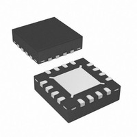
... Ordering Information Extended Type Number ATR7040-PVPG ATR7040-PVQG 10. Package Information Package: QFN 16 - 3x3 Exposed pad 1.7x1.7 (acc. JEDEC OUTLINE No. MO-220) Dimensions in mm Not indicated tolerances ±0. Drawing-No.: 6.543-5115.01-4 Issue: 1; 07.03.05 Assembly Chip PAC 4868C–DECT–05/06 Package Remarks QFN16, 3 × 3 Taped and reeled, MOQ 2000, Pb-free QFN16, 3 × ...
Page 8
... Disclaimer: The information in this document is provided in connection with Atmel products. No license, express or implied, by estoppel or otherwise, to any intellectual property right is granted by this document or in connection with the sale of Atmel products. EXCEPT AS SET FORTH IN ATMEL’S TERMS AND CONDI- TIONS OF SALE LOCATED ON ATMEL’S WEB SITE, ATMEL ASSUMES NO LIABILITY WHATSOEVER AND DISCLAIMS ANY EXPRESS, IMPLIED OR STATUTORY WARRANTY RELATING TO ITS PRODUCTS INCLUDING, BUT NOT LIMITED TO, THE IMPLIED WARRANTY OF MERCHANTABILITY, FITNESS FOR A PARTICULAR PURPOSE, OR NON-INFRINGEMENT ...