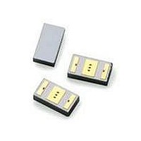
VMMK-2503-TR1G Avago Technologies US Inc., VMMK-2503-TR1G Datasheet

VMMK-2503-TR1G
Specifications of VMMK-2503-TR1G
Available stocks
Related parts for VMMK-2503-TR1G
VMMK-2503-TR1G Summary of contents
Page 1
... VMMK-2503 GHz GaAs Wideband Amplifier in Wafer Level Package Data Sheet Description Avago’s VMMK-2503 is an easy-to-use broadband, high linearity amplifier in a miniaturized wafer level package (WLP). The wide band and unconditionally stable perfor- mance makes this amplifier suitable as a gain block or a transmitter driver in many applications from 1– ...
Page 2
Table 1. Absolute Maximum Ratings Sym Parameters/Condition Vd Supply Voltage (RF Output) Id Device Current Input Power (RF Input) in, max P Total Power Dissipation diss Tch Max channel temperature T Storage Temperature STG Tjc Thermal ...
Page 3
Product Consistency Distribution Charts at 6.0 GHz 5V, Mean=68mA, USL=88mA Gain @ 6GHz, Mean=13.5dB, LSL=12.5dB, USL=18dB Note: Distribution data based on ~50Kpcs sample size from MPV lots. 3 NF@ 6GHZ, Mean=3.04dB, USL=4.1dB ...
Page 4
... VMMK-2503 Typical Performance (T = 25°C, Vdd = 5V, Idd = 65mA Frequency (GHz) [1] Figure 1. Small-signal Gain 0 -5 -10 -15 - Frequency (GHz) [1] Figure 3. Input Return Loss 0 -10 -20 - Frequency (GHz) [1] Figure 5. Output Return Loss Notes: 1. Data taken on a G-S-G probe substrate fully de-embedded to the reference plane of the package 2 ...
Page 5
... VMMK-2503 Typical Performance (continue 25°C, Vdd = 5V, Idd = 65mA 4. Frequency (GHz) [1] Figure 7. Gain over Vdd 0 -10 -20 5V 4. Frequency (GHz) [1] Figure 9. Input Return Loss over Vdd 0 -10 -20 - Frequency (GHz) [1] Figure 11. Output Return Loss Over Vdd Note: 1. Data taken on a G-S-G probe substrate fully de-embedded to the reference plane of the package ...
Page 6
... VMMK-2503 Typical Performance (continue 25°C, Vdd = 5V, Idd = 65mA 4. Frequency (GHz) [3] Figure 13. Output P1dB over Temp 25C 5 85C -40C Frequency (GHz) [3] Figure 15. Gain over Temp 0 -10 -20 - Frequency (GHz) [3] Figure 17. Input Return Loss Over Temp Notes: 1. Data taken on a G-S-G probe substrate fully de-embedded to the reference plane of the package 2 ...
Page 7
... VMMK-2503 Typical S-parameters (T = 25°C, Vdd = 5V, Idd = 65mA S11 Freq GHz Mag dB Phase 1 0.32 -9.94 -58.82 2 0.19 -14.31 -63.36 3 0.16 -15.75 -62.41 4 0.17 -15.65 -68.23 5 0.17 -15.19 -75.79 6 0.18 -14.78 -87.11 7 0.19 -14.44 -99.64 8 0.20 -14.12 -114.81 9 0.20 -14.04 -131.20 10 0.20 -13 ...
Page 8
... Figure 19. The recommended drain supply voltage and the corresponding drain current is approximately 65mA. The input of the VMMK-2503 is AC coupled and a DC-blocking capacitor is not required. Aspects of the amplifier perfor- mance may be improved over a narrower bandwidth by application of additional conjugate, linearity, or low noise (*opt) matching ...
Page 9
... Notes: 1. 0.010” Rogers RO4350 9 Recommended SMT Attachment The VMMK Packaged Devices are compatible with high volume surface mount PCB assembly processes. Manual Assembly for Prototypes 1. Follow ESD precautions while handling packages. 2. Handling should be along the edges with tweezers or from topside if using a vacuum collet ...
Page 10
... Ordering Information Devices Per Part Number Container VMMK-2503-BLKG 100 VMMK-2503-TR1G 5000 Package Dimension Outline Note: All dimensions are in mm Reel Orientation REEL USER FEED DIRECTION CARRIER TAPE 10 Container Antistatic Bag 7” Reel Symbol Min (mm) Max (mm) E 0.500 0.566 D 1.004 1.066 A 0.235 ...
Page 11
Tape Dimensions Note R0.1 5° (Max) Scale 5:1 AA SECTION Unit: mm Symbol Spec. K1 – Po 4.0±0.10 P1 4.0±0.10 P2 2.0±0.05 Do 1.55±0.05 D1 0.5±0.05 E 1.75±0.10 F 3.50±0.05 10Po 40.0±0.10 W ...


