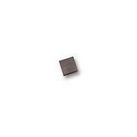
ACPM-7833-BLK Avago Technologies US Inc., ACPM-7833-BLK Datasheet - Page 18

ACPM-7833-BLK
Manufacturer Part Number
ACPM-7833-BLK
Description
IC PA MOD CDMA1900 PCS 8-SMD
Manufacturer
Avago Technologies US Inc.
Type
Power Amplifierr
Datasheet
1.ACPM-7833-TR1.pdf
(20 pages)
Specifications of ACPM-7833-BLK
Current - Supply
520mA
Frequency
1.85GHz ~ 1.91GHz
Gain
27.5dB
Noise Figure
4.5dB
Package / Case
10-SMD Module
Rf Type
CDMA
Voltage - Supply
3.2V ~ 4.2V
Operating Frequency
1910 MHz
Supply Current
550 mA
Maximum Power Dissipation
2500 mW
Maximum Operating Temperature
+ 85 C
Mounting Style
SMD/SMT
Minimum Operating Temperature
- 30 C
Number Of Channels
1 Channel
Frequency (max)
1.91GHz
Power Supply Requirement
Single
Single Supply Voltage (min)
3.2V
Single Supply Voltage (typ)
3.3V
Single Supply Voltage (max)
4.2V
Package Type
SMT
Dual Supply Voltage (min)
Not RequiredV
Dual Supply Voltage (typ)
Not RequiredV
Dual Supply Voltage (max)
Not RequiredV
Operating Temperature Classification
Commercial
Operating Temp Range
-30C to 85C
Pin Count
10
Mounting
Surface Mount
Lead Free Status / RoHS Status
Lead free / RoHS Compliant
P1db
-
Test Frequency
-
Lead Free Status / Rohs Status
Compliant
2) Circuit Operation
The design of the power module (PAM) provide bias
control via Vcntl to achieve optimal RF performance
and power control. The control pin is labeled Vcntl.
Please refer to for the block diagram of this PAM.
Typical Operation Conditions
(Vdd1=Vdd2=Vbias = 3.4V)
Parameter
Frequency Range
Output Power
Vcntl
3) Maximum Ratings
4) Heat Sinking
5) Testing
Figure 24. Power Module Block Diagram.
18
Input
Vdd 5.0V
Drain Current 1.5A
Vcntl 3V
RF input
Temperature -30 to 85°C
Please Note: Avoid Electrostatic Discharge on all I/
O’s.
The demonstration PC Board provides an adequate
heat sink. Maximum device dissipation should be
kept below 2.5 Watts.
- Signal Source
The CDMA modulated signal for the test is generated
using an Agilent ESG-D4000A (or ESG-D3000A)
Digital Signal Generator with the following settings:
CDMA Setup : Reverse
Spreading: On
Bits/Symbol: 1
Data: PN15
Modulation: OQPSK
Chip Rate: 1.2288 Mcps
Passive
Match
Input
10 dBm
ACPM-7833
1850 – 1910 MHz
28.5 dBm
2.5 V
Vdd1
Bias Circuit
Inter-stage
On Chip
Vbias
Match
Vcntl
Single control bias setting for low Idq
and 40% PAE at Pout = 28.5 dBm
Vdd2
Passive
Output
Match
High Crest: On
Filter: Std
Phase Polarity: Invert
- ACPR Measurement
The ACPR (and channel power) is measured using
an
corresponding ACPR offsets for IS-98c and JSTD-8.
Averaging of 10 is used for ACPR measurements.
- DC Connection
A DC connector is provided to allow ease of
connection to the I/Os. Wires can be soldered to
the connector pins, or the connector can be
removed and I/Os contacted via clip leads or direct
soldered connections. The wiring of I/Os are listed
in Figures 20 through 23 and the Pin configuration
table. The Vdd sense connections are provided to
allow the use of remote-sensing power supplies of
compensation for PCB traces and cable resistance.
- Device Operation
1) Connect RF Input and Output for the band under
2) Terminate all unused RF ports into 50 Ohms.
3)
4) Connect Vcntl supply and set reference voltage
5) Apply RF input power according to the values
6) Power down in opposite sequence.
test.
(including remote sensing labeled Vdd1 S, Vdd2
S and Vbias S on the board). Nominal voltage is
3.4V.
to the voltage shown in the data packet. Note
that the Vcntl pin is on the back side of the
demonstration board. Please limit Vcntl to not
exceed the corresponding listed “DC Biasing
Condition” in the Data Packet. Note that
increasing Vcntl over the corresponding listed
“DC Biasing Condition” can result in power
decrease and current can exceed the rated limit.
listed in “Operation Data” in Data Packet.
Connect Vdd1, Vdd2 and Vdd3 supplies
Avago
Output
Technologies
4406
VSA
with


