AMMP-6130-BLKG Avago Technologies US Inc., AMMP-6130-BLKG Datasheet

IC MMIC PWR AMP 30GHZ 8SMD

AMMP-6130-BLKG

Manufacturer Part Number
AMMP-6130-BLKG
Description
IC MMIC PWR AMP 30GHZ 8SMD
Manufacturer
Avago Technologies US Inc.
Type
Power Amplifierr
Datasheet

Specifications of AMMP-6130-BLKG

Gain
18.5dB
Current - Supply
200mA
Frequency
15GHz, 30GHz
Package / Case
8-SMD
Rf Type
VSAT, DBS
Voltage - Supply
3.5 V ~ 5 V
Supply Current
200mA
Supply Voltage Range
3.5V To 5V
Rf Ic Case Style
SMD
No. Of Pins
8
Operating Temperature Range
-65°C To +150°C
Termination Type
SMD
Number Of Channels
1
Power Supply Requirement
Single
Single Supply Voltage (min)
3.5V
Single Supply Voltage (typ)
4.5V
Single Supply Voltage (max)
5V
Package Type
SMT
Dual Supply Voltage (min)
Not RequiredV
Dual Supply Voltage (typ)
Not RequiredV
Dual Supply Voltage (max)
Not RequiredV
Pin Count
8
Mounting
Surface Mount
Filter Terminals
SMD
Rohs Compliant
Yes
Lead Free Status / RoHS Status
Lead free / RoHS Compliant
Noise Figure
-
P1db
-
Test Frequency
-
Lead Free Status / Rohs Status
Compliant
AMMP-6130
30 GHz Power Amplifier with Frequency Multiplier (x2)
in SMT Package
Data Sheet
Description
Avago Technologies AMMP-6130 is a high gain, narrow-
band doubler and output power amplifier designed for
DBS applications and other commercial communication
systems. The MMIC takes an input 15 GHz signal and
passes it through a harmonic frequency multiplier (x2)
and then three stages of power amplification. Integrated
matching structures filter and match input/output to
50 Ω. It has integrated input and output DC blocking
capacitors and bias structures to all stages. The MMIC is
fabricated using PHEMT technology. The backside of this
package part is both RF and DC ground. This helps sim-
ply the assembly process and reduces assembly related
performance variations and costs. The surface mount
package allows elimination of “chip & wire” assembly
for lower cost. This MMIC is a cost effective alternative
to hybrid (discrete-FET) amplifiers that require complex
tuning and assembly process.
Pin Connections (Top View)
8
X2
1
7
2
6
Note: These devices are ESD sensitive. The following precautions are strongly recommended. Ensure
that an ESD approved carrier is used when units are transported from one destination to another.
Personal grounding is to be worn at all times when handling these devices. The manufacturer assumes
no responsibilities for ESD damage due to improper storage and handling of these devices.
3
5
GND
PACKAGE
BASE
4
Pin
1
2
3
4
5
6
7
8
Function
V
RF
RF
d
Out
In
Features
• Surface Mount Package, 5.0 x 5.0 x 1.25 mm
• Integrated DC Block and Choke
• 50 Ω Input and Output Match
• Single Positive Supply Pin
• No Negative Gate Bias
Specifications (Vd=4.5V, Idd=200mA)
• Frequency Range 15GHz in, 30GHz out
• Output Power: 21 dBm
• Harmonic Suppression: 60dBc
• Single Positive Supply
• DC Requirements: 4.5V, 200mA
Applications
• Microwave Radio systems
• Satellite VSAT, DBS Up/Down Link
• Broadband Wireless Access)

Related parts for AMMP-6130-BLKG

AMMP-6130-BLKG Summary of contents

Page 1

... GHz Power Amplifier with Frequency Multiplier (x2) in SMT Package Data Sheet Description Avago Technologies AMMP-6130 is a high gain, narrow- band doubler and output power amplifier designed for DBS applications and other commercial communication systems. The MMIC takes an input 15 GHz signal and passes it through a harmonic frequency multiplier (x2) and then three stages of power amplification ...

Page 2

... The absolute maximum ratings for Vdd, Idd and Pin were determined at an ambient temperature of 25°C unless noted otherwise. (4,5) AMMP-6130 RF Specifications TA= 25°C, Vdd = 4.5 V, Idd = 200mA, Zo=50 Ω, Pin=5dBm Symbol Parameters and Test Conditions Freq ...

Page 3

... AMMP-6130 Typical Performance (TA = 25°C, Vdd=4.5V, Idd=200 mA, Zin = Zout = 50Ω, Pin=3dBm unless otherwise stated C.G. 2H- 14.5 15 15.5 Input Frequency [GHz] Figure 1. Conversion Gain & Fundamental Sup vs. Input Freq 3. 4. 29.5 30 Frequency [GHz] Figure 3. Output Power vs. Output Frequency @ 4 bias levels Pin [dBm] Figure 5 ...

Page 4

Typical Scattering Parameters [1] (TA = 25°C, Vdd =4.5 V, IDD = 200 mA, Zin = Zout = 50 Ω) Freq S11 GHz dB Mag Phase dB 1 -2.166 0.779 73.909 -80.000 2 -2.531 0.747 -33.368 -55.139 3 -3.497 0.669 ...

Page 5

... The input also consists of matching components tuned to 15GHz. An additional LC-filter is included at the input for stability. The doubler is operated at pinch-off to create a half- wave conduction angle ideal for generation of the 2nd harmonic. The AMMP-6130 is also designed for stability over temperature. MLOC TL8 C ...

Page 6

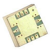
... Recommended SMT Attachment for 5x5 Package The AMMP Packaged Devices are compatible with high volume surface mount PCB assembly processes. The PCB material and mounting pattern, as defined in the data sheet, optimizes RF performance and is strongly recommended. An electronic drawing of the land pat- tern is available upon request from Avago Sales & Ap- plication Engineering ...

Page 7

... Peak = 250 ± 5˚C 250 200 150 100 50 Ramp 1 Preheat Ramp 2 Reflow 100 150 Seconds Figure 11. Suggested Lead-Free Reflow Profile for SnAgCu Solder Paste Package Dimensions AMMP XXXX YWWDNN FRONT VIEW SYMBOL MIN. MAX. A 0.198 (5.03) 0.213 (5.4) B 0.0685 (1.74) 0.088 (2.25) ...

Page 8

... AMMP AMMP XXXX XXXX AMMP-6130 Part Number Ordering Information Part Number Devices Per Container AMMP-6130-BLKG 10 AMMP-6130-TR1G 100 AMMP-6130-TR2G 500 Note performance degradation is seen due to ESD upto 250 V HBM and 80 V MM. The DC characteristics in general show increased leakage at lower ESD discharge voltages. The user is reminded that this device is ESD sensitive and needs to be handled with all necessary ESD protocols ...

Related keywords