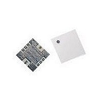
AMMP-6233-BLKG Avago Technologies US Inc., AMMP-6233-BLKG Datasheet - Page 5

AMMP-6233-BLKG
Manufacturer Part Number
AMMP-6233-BLKG
Description
IC MMIC LNA 18GHZ-31GHZ 8SMD
Manufacturer
Avago Technologies US Inc.
Type
Low Noise Amplifierr
Datasheet
1.AMMP-6233-TR2G.pdf
(8 pages)
Specifications of AMMP-6233-BLKG
Rf Type
VSAT, DBS
Gain
23.2dB
Current - Supply
65mA
Frequency
18GHz ~ 32GHz
Noise Figure
2.6dB
P1db
8dBm
Package / Case
8-SMD
Test Frequency
18GHz
Voltage - Supply
3 V ~ 5 V
Frequency Rf
32GHz
Noise Figure Typ
2.6dB
Supply Current
65mA
Supply Voltage Range
3V To 5V
Frequency Max
32GHz
Termination Type
SMD
Package
8SMD
Typical Output Power
8(Min)@29000MHz dBm
Typical Power Gain
23.6@29000MHz dB
Typical Output Intercept Point
18(Min)@29000MHz dBm
Maximum Output Return Loss
13(Min)@29000MHz dB
Maximum Input Return Loss
10(Min)@29000MHz dB
Maximum Supply Voltage
5 V
Number Of Channels
1
Frequency (max)
32GHz
Power Supply Requirement
Single
Single Supply Voltage (min)
3V
Single Supply Voltage (typ)
3V
Single Supply Voltage (max)
5V
Package Type
SMD
Dual Supply Voltage (min)
Not RequiredV
Dual Supply Voltage (typ)
Not RequiredV
Dual Supply Voltage (max)
Not RequiredV
Pin Count
8
Mounting
Surface Mount
Filter Terminals
SMD
Rohs Compliant
Yes
Frequency Min
18GHz
Lead Free Status / RoHS Status
Lead free / RoHS Compliant
Lead Free Status / RoHS Status
Lead free / RoHS Compliant, Lead free / RoHS Compliant
Available stocks
Company
Part Number
Manufacturer
Quantity
Price
Part Number:
AMMP-6233-BLKG
Manufacturer:
AVAGO/安华高
Quantity:
20 000
AMMP-6233 Application and Usage
Figure 13. Application of AMMP-6233
Figure 14. Evaluation / Test Board (Available to qualified customer re-
quests)
Figure 15. Simplified LNA Schematic
RFin
In
AMMP-6233
1
7
Vdd
2
6
3
5
0.1uF
RFout
Vcc
Biasing and Operation
The AMMP-6233 is normally biased with a positive drain
supply connected to the VDD pin through a 0.1uF bypass
capacitor as shown in Figure 13. The recommended drain
supply voltage is 3V. It is important to have 0.1uF bypass
capacitor, and the capacitor should be placed as close to
the component as possible. Input and output ports are
DC-blocked. Impedance matching at input and output
ports are achieved on-chip, therefore, no extra external
component is needed. Aspects of the amplifier perfor-
mance may be improved over a narrower bandwidth by
application of additional conjugate, linearity, or low noise
(Γopt) matching No ground wires are needed because all
ground connections are made with plated through-holes
to the backside of the package.
Refer the Absolute Maximum Ratings table for allowed
DC and thermal condition
Out


