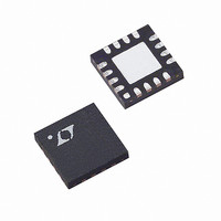
LT5506EUF Linear Technology, LT5506EUF Datasheet - Page 6

LT5506EUF
Manufacturer Part Number
LT5506EUF
Description
IC DEMOD QUADRATURE VGA 16QFN
Manufacturer
Linear Technology
Datasheet
1.LT5506EUF.pdf
(12 pages)
Specifications of LT5506EUF
Function
Demodulator
Lo Frequency
80MHz ~ 1GHz
Rf Frequency
40MHz ~ 500MHz
Gain
59dB
Noise Figure
6.8dB
Current - Supply
36mA
Voltage - Supply
1.8 V ~ 5.25 V
Package / Case
16-QFN
Lead Free Status / RoHS Status
Contains lead / RoHS non-compliant
P1db
-
Available stocks
Company
Part Number
Manufacturer
Quantity
Price
Part Number:
LT5506EUF
Manufacturer:
LINEAR/凌特
Quantity:
20 000
Company:
Part Number:
LT5506EUF#PBF
Manufacturer:
LT
Quantity:
3 360
Part Number:
LT5506EUF#PBF
Manufacturer:
LINEAR/凌特
Quantity:
20 000
Company:
Part Number:
LT5506EUF#TRPBF
Manufacturer:
ST
Quantity:
10 439
Part Number:
LT5506EUF#TRPBF
Manufacturer:
LINEAR/凌特
Quantity:
20 000
PI FU CTIO S
GND (Pins 1, 4, 17): Ground. Pins 1 and 4 are connected
to each other internally. The Exposed Pad (Pin 17) is not
connected internally to Pins 1 and 4. For chip functionality,
the Exposed Pad and either Pin 1 or Pin 4 must be
connected to ground. For best RF performance, Pin 1,
Pin 4 and the Exposed Pad should be connected to RF
ground.
IF
Each pin must be DC grounded through an external
inductor or RF transformer with central ground tap. This
path should have a DC resistance lower than 2 to ground.
V
decoupled to ground using 1000pF and 0.1 F capacitors.
V
the IF gain and its typical input voltage range is 0.2V to
1.7V. It is internally biased via a 25k resistor to 0.2V,
setting a low gain if the V
IF
signals, the DC level at this pin is a function of the IF input
signal level.
LT5506
(Note 5), f
unless otherwise noted. (Note 3)
TYPICAL PERFOR A CE CHARACTERISTICS
6
CC
CTRL
+
1.4
1.2
1.0
0.8
0.6
0.4
0.2
DET
, IF
U
(Pins 5 and 8): Power Supply. These pins should be
–40
IF Detector Output Voltage
vs IF Input CW Power and
Supply Voltage
f
–
(Pin 6): VGA Gain Control Input. This pin controls
IF
(Pin 7): IF Detector Output. For strong IF input
= 280MHz
(Pins 2, 3): Differential Inputs for the IF Signal.
IF
–30
U
= 284MHz, P
IF INPUT CW POWER (dBm)
–20
U
IF
–10
3V
= –30dBm, I and Q outputs 800mV
CTRL
5.25V
1.8V
W
0
pin is left floating.
5506 G16
U
10
1.6
1.4
1.2
1.0
0.8
0.4
0.2
0.6
–40
IF Detector Output Voltage vs IF
Input CW Power and IF Frequency
V
CC
= 3V
–30
IF INPUT CW POWER (dBm)
P-P
into 4k differential load, T
–20
f
f
IF
IF
EN (Pin 9): Enable Input. When the enable pin voltage is
higher than 1V, the IC is completely turned on. When the
input voltage is less than 0.5V, the IC is turned off, except
the part of the circuit associated with standby mode.
2xLO
2xLO Input. The 2xLO input frequency must be twice that
of the IF frequency. The internal bias voltage is V
STBY (Pin 12): Standby Input. When the STBY pin is
higher than 1V, the standby mode circuit is turned on to
prebias the I/Q buffers. When the STBY pin is less than
0.5V, the standby mode circuit is turned off.
Q
puts of the Q Channel. Internally biased at V
I
of the I Channel. Internally biased at V
OUT
= 550MHz
= 280MHz
OUT
–10
–
–
–
, I
, Q
f
, 2xLO
IF
OUT
= 40MHz
0
OUT
+
5506 G17
V
(Pins 15, 16): Differential Baseband Outputs
+
+
CC
10
(Pins 13, 14): Differential Baseband Out-
(Pins 10, 11): Differential Inputs for the
= 3V. f
A
2 LO
= 25 C, EN = V
95
94
93
92
91
90
89
88
–20
= 570MHz, P
Phase Relation Between I and Q
Outputs vs LO Input Power
–15
LO INPUT POWER (dBm)
CC
–10
, STBY = V
2 LO
CC
–5
= –5dBm
– 1.19V.
f
f
f
f
f
IF
IF
IF
IF
IF
= 284MHz, 25 C
= 284MHz, –40 C
= 284MHz, 85 C
= 40MHz, 25 C
= 550MHz, 25 C
CC
CC
0
CC
– 1.19V.
,
– 0.4V.
5
5506 G18
5506fa
10


