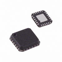
ADL5382ACPZ-R7 Analog Devices Inc, ADL5382ACPZ-R7 Datasheet - Page 18

ADL5382ACPZ-R7
Manufacturer Part Number
ADL5382ACPZ-R7
Description
IC DEMOD QUAD 700M2.7GHZ 24LFCSP
Manufacturer
Analog Devices Inc
Datasheet
1.ADL5382ACPZ-R7.pdf
(28 pages)
Specifications of ADL5382ACPZ-R7
Design Resources
Interfacing ADL5382 to AD9262 as an RF-to-Bits Solution (CN0062)
Function
Demodulator
Lo Frequency
700MHz ~ 2.7GHz
Rf Frequency
700MHz ~ 2.7GHz
P1db
14.5dBm
Gain
3.3dB
Noise Figure
17.6dB
Current - Supply
220mA
Voltage - Supply
4.75 V ~ 5.25 V
Package / Case
24-VFQFN, 24-CSP Exposed Pad
Frequency Range
700MHz To 2.7GHz
Rf Type
Quadrature
Supply Voltage Range
4.75V To 5.25V
Rf Ic Case Style
LFCSP
No. Of Pins
24
Operating Temperature Range
-40°C To +85°C
Lead Free Status / RoHS Status
Lead free / RoHS Compliant
Other names
ADL5382ACPZ-R7TR
Available stocks
Company
Part Number
Manufacturer
Quantity
Price
Company:
Part Number:
ADL5382ACPZ-R7
Manufacturer:
Analog Devices Inc
Quantity:
1 881
Part Number:
ADL5382ACPZ-R7
Manufacturer:
ADI/亚德诺
Quantity:
20 000
ADL5382
As an example, a second-order Butterworth, low-pass filter
design is shown in Figure 50 where the differential load impedance
is 500 Ω and the source impedance of the ADL5382 is 50 Ω. The
normalized series inductor value for the 10-to-1, load-to-source
impedance ratio is 0.074 H, and the normalized shunt capacitor
is 14.814 F. For a 10.9 MHz cutoff frequency, the single-ended
equivalent circuit consists of a 0.54 μH series inductor followed
by a 433 pF shunt capacitor.
The balanced configuration is realized as the 0.54 μH inductor
is split in half to realize the network shown in Figure 50.
A complete design example is shown in Figure 53. A sixth-order
Butterworth differential filter having a 1.9 MHz corner frequency
interfaces the output of the ADL5382 to that of an ADC input.
The 500 Ω load resistor defines the input impedance of the
ADC. The filter adheres to typical direct conversion W-CDMA
applications, where 1.92 MHz away from the carrier IF frequency,
1 dB of rejection is desired and 2.7 MHz away 10 dB of rejection
is desired.
V
V
V
S
S
S
Figure 50. Second-Order Butterworth, Low-Pass Filter Design Example
R
R
S
L
= 0.1
R
R
R
R
S
2
2
S
S
S
= 50Ω
= 50Ω
= 25Ω
= 25Ω
CONFIGURATION
CONFIGURATION
DENORMALIZED
SINGLE-ENDED
SINGLE-ENDED
NORMALIZED
EQUIVALENT
L
BALANCED
N
0.54µH
0.27µH
0.27µH
= 0.074H
C
N
14.814F
433pF
433pF
f
C
f
R
R
R
C
R
2
2
= 10.9MHz
L
L
L
L
= 1Hz
= 500Ω
= 500Ω
= 250Ω
= 250Ω
Rev. 0 | Page 18 of 28
Figure 51 and Figure 52 show the measured frequency response
and group delay of the filter.
–10
–15
–20
900
800
700
600
500
400
300
200
100
10
–5
5
0
0
0
Figure 52. Sixth-Order Baseband Filter Group Delay
Figure 51. Sixth-Order Baseband Filter Response
0.2
0.5
0.4
1.0
0.6
FREQUENCY (MHz)
FREQUENCY (MHz)
1.5
0.8
1.0
2.0
1.2
2.5
1.4
1.6
3.0
1.8
3
.5


