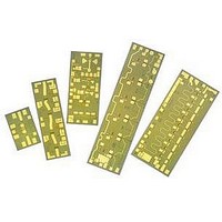
AMMC-5023-W50 Avago Technologies US Inc., AMMC-5023-W50 Datasheet - Page 7

AMMC-5023-W50
Manufacturer Part Number
AMMC-5023-W50
Description
IC MMIC AMP LO NOISE 23GHZ
Manufacturer
Avago Technologies US Inc.
Type
General Purposer
Datasheet
1.AMMC-5023-W50.pdf
(9 pages)
Specifications of AMMC-5023-W50
Function
Amplifier
Gain
23dB
Noise Figure Typ
2.3dB
Supply Current
28mA
Supply Voltage Range
3V To 7V
Frequency Max
26.5GHz
Frequency Min
21.2GHz
Supply Voltage Max
7V
Supply Voltage Min
3V
Number Of Channels
1
Frequency (max)
26.5GHz
Output Power
10@26500MHzdBm
Power Supply Requirement
Single
Single Supply Voltage (min)
3V
Single Supply Voltage (typ)
5V
Single Supply Voltage (max)
7V
Dual Supply Voltage (min)
Not RequiredV
Dual Supply Voltage (typ)
Not RequiredV
Dual Supply Voltage (max)
Not RequiredV
Operating Temperature Classification
Military
Operating Temp Range
-55C to 140C
Lead Free Status / RoHS Status
Lead free / RoHS Compliant
Lead Free Status / RoHS Status
Lead free / RoHS Compliant, Lead free / RoHS Compliant
Biasing and Operation
The AMMC-5023 has four cascaded gain stages as shown
in Figure 19. The first two gain stages at the input are
biased with the V
stages are biased with the V
eration is with a single positive DC drain supply voltage
(V
2(a).
If desired, the output stage DC supply voltage (V
be increased to improve output power capability while
maintaining optimum low noise bias conditions for the
input section. The output power may also be adjusted
by applying a positive voltage at V
ing bias point for both the output FETs. Increasing the
voltage applied to V
negative gate-to-source voltage and, therefore, lower
drain current. Figures 20(b) and 20(c) illustrate how the
device can be assembled for independent drain supply
operation and for output stage gate bias control.
RF Input
Figure 19. AMMC-5023 Schematic.
7
D1
=V
D2
=5 V) as shown in the assembly diagram, Figure
D1
drain supply. Similarly, the two output
V
G1
G2
(more positively) results in a more
D2
supply. Standard LNA op-
G2
to alter the operat-
V
D1
D2
) can
Assembly Techniques
The backside of the MMIC chip is RF ground. For mi-
crostrip applications the chip should be attached directly
to the ground plane (e.g. circuit carrier or heatsink) using
electrically conductive epoxy
the amount should be just enough to provide a thin fillet
around the bottom perimeter of the die. The ground
plane should be free of any residue that may jeopardize
electrical or mechanical attachment. Caution should be
taken to not exceed the Absolute Maximum Rating for
assembly temperature and time.
Thermosonic wedge bonding is the preferred method for
wire attachment to the bond pads. The RF connections
should be kept as short as possible to minimize induc-
tance. Gold mesh or double-bonding with 0.7 mil gold
wire is recommended.
Mesh can be attached using a 2 mil round tracking tool
and a tool force of approximately 22 grams with an ultra-
sonic power of roughly 55 dB for a duration of 76 ± 8 mS.
A guided wedge at an ultrasonic power level of 64 dB can
be used for the 0.7 mil wire. The recommended wire bond
stage temperature is 150 ± 2°C.
The chip is 100 mm thick and should be handled with
care. This MMIC has exposed air bridges on the top
surface. Handle at edges or with a custom collet (do not
pick up die with vacuum on die center.)
This MMIC is also static sensitive and ESD handling pre-
cautions should be taken.
Notes:
1. Ablebond 84-1 LM1 silver epoxy is recommended.
2. Eutectic attach is not recommended and may jeopardize reliability
of the device.
V
G2
V
D2
[1,2]
. For conductive epoxy,
RF Output


