RF5110GPCK-410 RFMD, RF5110GPCK-410 Datasheet - Page 2
RF5110GPCK-410
Manufacturer Part Number
RF5110GPCK-410
Description
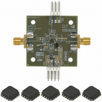
KIT EVAL FOR RF5110G
Manufacturer
RFMD
Type
Amplifierr
Datasheet
1.RF5110GTR7.pdf
(22 pages)
Specifications of RF5110GPCK-410
Frequency
800MHz ~ 950MHz
For Use With/related Products
RF5110G
Lead Free Status / RoHS Status
Lead free / RoHS Compliant
Other names
689-1054
RF5110GPCBA-410
RF5110GPCBA-410
Available stocks
Company
Part Number
Manufacturer
Quantity
Price
Company:

Part Number:
RF5110GPCK-410
Manufacturer:
RFMD
Quantity:
5 000


RF5110G
2 of 22
Absolute Maximum Ratings
Supply Voltage
Power Control Voltage (V
DC Supply Current
Input RF Power
Duty Cycle at Max Power
Output Load VSWR
Operating Case Temperature
Storage Temperature
Overall
Operating Frequency Range
Usable Frequency Range
Maximum Output Power
Total Efficiency
Input Power for Max Output
Output Noise Power
Forward Isolation
Second Harmonic
Third Harmonic
All Other Non-Harmonic
Input Impedance
Optimum Source Impedance
Input VSWR
Output Load VSWR
Output Load Impedance
Spurious
Parameter
Parameter
Ruggedness
APC1,2
Stability
)
7628 Thorndike Road, Greensboro, NC 27409-9421 · For sales or technical
support, contact RFMD at (+1) 336-678-5570 or sales-support@rfmd.com.
Min.
33.8
33.1
+4.5
10:1
8:1
50
-0.5 to +6.0
-0.5 to +3.0
-55 to +150
-40 to +85
Rating
2400
10:1
Specification
+13
50
800 to 950
880 to 915
2.6-j1.5
40+j10
Typ.
34.5
+7.0
-20
-25
57
12
50
5
Max.
2.5:1
Unit
+9.5
dBm
V
-72
-81
-22
-36
4:1
mA
°C
°C
-7
-7
%
DC
V
Exceeding any one or a combination of the Absolute Maximum Rating conditions may
cause permanent damage to the device. Extended application of Absolute Maximum
Rating conditions to the device may reduce device reliability. Specified typical perfor-
mance or functional operation of the device under Absolute Maximum Rating condi-
tions is not implied.
RoHS status based on EUDirective2002/95/EC (at time of this document revision).
The information in this publication is believed to be accurate and reliable. However, no
responsibility is assumed by RF Micro Devices, Inc. ("RFMD") for its use, nor for any
infringement of patents, or other rights of third parties, resulting from its use. No
license is granted by implication or otherwise under any patent or patent rights of
RFMD. RFMD reserves the right to change component circuitry, recommended appli-
cation circuitry and specifications at any time without prior notice.
Unit
dBm
dBm
dBm
dBm
dBm
dBm
dBm
dBm
dBm
MHz
MHz
%
%
%
Ω
Ω
Ω
Caution! ESD sensitive device.
Temp=25°C, V
P
37.5% Duty Cycle, pulse width=1731μs
See evaluation board schematic.
Using different evaluation board tune.
Temp=+60°C, V
At P
P
P
RBW=100kHz, 925MHz to 935MHz,
P
P
RBW=100kHz, 935MHz to 960MHz,
P
P
P
P
For best noise performance
P
P
Spurious<-36dBm, V
RBW=100kHz
No damage
Load Impedance presented at RF OUT pad
Temp=25°C, V
V
OUT
OUT
OUT,MIN
OUT,MIN
APC1,2
OUT,MAX
OUT
IN
IN,MIN
IN,MIN
IN
IN
=+9.5dBm
=+9.5dBm
=+4.5dBm, Freq=880MHz to 915MHz,
OUT,MAX
<P
=+20dBm
=+10dBm
<P
<P
=0.3V, P
OUT,MAX
<P
<P
-5dB<P
IN
IN
OUT
OUT
, V
<P
<P
CC
CC
CC
IN,MAX
IN,MAX
CC
<P
<P
IN
-5dB
Condition
OUT
=3.6V
=3.6V, V
=3.6V, V
=+9.5dBm
=3.3V, V
OUT,MAX
OUT,MAX
APC1,2
<P
, V
, V
CC
CC
OUT,MAX
APC1,2
APC1,2
=0.3V to 2.6V,
=3.3V to 5.0V
=3.3V to 5.0V
APC1,2
,
,
Rev A4 DS071026
=2.8V,
=2.8V
=2.8V
Related parts for RF5110GPCK-410
Image
Part Number
Description
Manufacturer
Datasheet
Request
R

Part Number:
Description:
3V GSM POWER AMPLIFIER
Manufacturer:
RF Micro Devices
Datasheet:

Part Number:
Description:
IC AMP HBT GAAS CATV 8-SOIC
Manufacturer:
RFMD
Datasheet:

Part Number:
Description:
IC AMP MMIC GAAS 12GHZ 4-MICROX
Manufacturer:
RFMD
Datasheet:

Part Number:
Description:
IC AMP 3V LOW-NOISE SOT23-6
Manufacturer:
RFMD
Datasheet:

Part Number:
Description:
KIT EVAL FOR NBB-310
Manufacturer:
RFMD
Datasheet:
Part Number:
Description:
IC AMPLIFIER MMIC LNA 8-QFN
Manufacturer:
RFMD
Datasheet:
Part Number:
Description:
IC AMP MMIC GAAS 4GHZ 4-MICROX
Manufacturer:
RFMD
Datasheet:
Part Number:
Description:
IC SWITCH 10W PHEMT SPDT 12QFN
Manufacturer:
RFMD
Datasheet:
Part Number:
Description:
IC QUADRATURE MODULATOR 16-SOIC
Manufacturer:
RFMD
Datasheet:
Part Number:
Description:
100MHZ TO 4000MHZ, GAAS PHEMT MMIC LOW NOISE AMPLIFIERS
Manufacturer:
RFMD
Part Number:
Description:
KIT EVAL FOR RF2336
Manufacturer:
RFMD
Datasheet:


Part Number:
Description:
IC AMP WLAN/LNA DVR 3V SOT23-5
Manufacturer:
RFMD
Datasheet:

Part Number:
Description:
IC AMP HBT GAAS LNA BYPASS 8-QFN
Manufacturer:
RFMD
Datasheet: