RF5110GPCK-410 RFMD, RF5110GPCK-410 Datasheet - Page 6
RF5110GPCK-410
Manufacturer Part Number
RF5110GPCK-410
Description
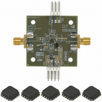
KIT EVAL FOR RF5110G
Manufacturer
RFMD
Type
Amplifierr
Datasheet
1.RF5110GTR7.pdf
(22 pages)
Specifications of RF5110GPCK-410
Frequency
800MHz ~ 950MHz
For Use With/related Products
RF5110G
Lead Free Status / RoHS Status
Lead free / RoHS Compliant
Other names
689-1054
RF5110GPCBA-410
RF5110GPCBA-410
Available stocks
Company
Part Number
Manufacturer
Quantity
Price
Company:

Part Number:
RF5110GPCK-410
Manufacturer:
RFMD
Quantity:
5 000


RF5110G
General Purpose Radio Applications
RF5110G has seen widespread use in GSM handset applications, but it can also be used as a final transmit PA for general pur-
pose radio (FSK, ASK). The application schematics in this data sheet outline matching for commonly used frequency bands.
Matching is shown for 150MHz, 220MHz, 450MHz, and 865MHz to 928MHz. The standard 900MHz GSM evaluation board
can be easily converted for these bands, using the values indicated. The 865MHZ to 928MHz conversion is the most direct,
with adjustment required only on output match. The others show changes at input, 1st interstage, 2nd interstage, and output.
Common components can be used in most cases. The only key component is the choke seen on RF output. During develop-
ment of the matches, one goal was to achieve stability (no spurious) into 5:1 output VSWR. The 1μH value and construction
proved essential in achieving this level of stability.
This Theory of Operation applies to an open loop system utilizing no power control. In the traditional GSM application, power is
sampled at the RF5110G’s output and fed back to a log detect function. DAC voltage (V
detector output drives the V
power>0dBm applied. Power can be set over the full range of defined levels, ranging from small signal to compression. In
addition, the control loop is used for ramping in accordance with GSM specifications. If power control is used in the system
under consideration, most of the open loop constraints covered here will not apply, aside from thermal considerations dis-
cussed below.
When used in an open loop system, RF5110G should be operated in compression. When running small signal, some variation
in gain (and therefore output power) will be seen over temperature extremes between -40°C and 85°C. When operated in com-
pression, the impact of this variation is substantially mitigated, making open loop application practical. “Compression” in this
case is defined where efficiency exceeds 45%. In the graph section of this data sheet, curves in each frequency band are
shown for gain/efficiency/junction temperature versus P
compressed output power with appropriate choice of supply voltage (V
Operation at 31dBm shows efficiency=49% for V
efficiency. So, the system designer can choose an appropriate supply voltage which provides high efficiency at target P
One important detail to consider is voltage level at V
trol loop. This voltage controls output power from the PA. In open loop mode, V
output power from RF5110G in volume production.
Another design consideration is maintaining acceptable junction temperature. In the GSM radio, output power in excess of
34dBm is common. This is allowable due to the limit on transmit duty cycle and pulse width. The worst case condition sees
duty cycle at 50%, with pulse width equal to approximately 2msec. In this situation, the PA cuts off before junction temperature
reaches the maximum that would be seen with longer pulse width. For the non–GSM radio, it is assumed pulse width will
exceed 2msec. Thus, restrictions must be imposed on allowable maximum output power. The most conservative analysis is
used, that for 100% duty cycle. Thermal scans have shown R
36°C/W. R
curves show projected junction temperatures (T
ation board is taken into account. A conservative goal is T
ture of 85°C. Maximum output power will then be bounded by that limit. Observing the T
928MHz, one sees that 32dBm is always at or below 150°C. This shows that the output load line in each match was intention-
ally set for high efficiency. To ensure equivalent performance in one’s system, care should be taken to achieve efficiency equal
to or better than that seen in the data. Thermal performance can be predicted with a simple calculation at a desired output
power:
6 of 22
P_DC=V
P
OUT
(Watt)=[10^(P
TH
CC
for the evaluation board has been calculated at 10.4°C/W, giving RF5110G R
xI
CC
OUT
APC
(dBm)/10)]/1000
7628 Thorndike Road, Greensboro, NC 27409-9421 · For sales or technical
support, contact RFMD at (+1) 336-678-5570 or sales-support@rfmd.com.
pin of RF5110G such that output power corresponding to V
Theory of Operation
J
) for each general purpose radio frequency band. R
CC
=2.8V. If 32dBm output is required in design, using V
APC
. As noted earlier, V
OUT
J
≤150°C when operating at a maximum specified ambient tempera-
/V
TH
CC
. As indicated in the graphs, high efficiency can be obtained at
(thermal resistance) of RF5110G+the evaluation board to be
CC
). For example, see the efficiency curves for 450MHz.
APC
level varies when operating within a power con-
APC
should be set at 2.8V to ensure consistent
SET
) is also input to the log detector. Log
SET
J
curves in bands from 150MHz to
is obtained, with constant input
TH_JC
TH
=25.6°C/W. Data sheet
of RF5110G+the evalu-
CC
=3.3V gives 47%
Rev A4 DS071026
OUT
.
Related parts for RF5110GPCK-410
Image
Part Number
Description
Manufacturer
Datasheet
Request
R

Part Number:
Description:
3V GSM POWER AMPLIFIER
Manufacturer:
RF Micro Devices
Datasheet:

Part Number:
Description:
IC AMP HBT GAAS CATV 8-SOIC
Manufacturer:
RFMD
Datasheet:

Part Number:
Description:
IC AMP MMIC GAAS 12GHZ 4-MICROX
Manufacturer:
RFMD
Datasheet:

Part Number:
Description:
IC AMP 3V LOW-NOISE SOT23-6
Manufacturer:
RFMD
Datasheet:

Part Number:
Description:
KIT EVAL FOR NBB-310
Manufacturer:
RFMD
Datasheet:
Part Number:
Description:
IC AMPLIFIER MMIC LNA 8-QFN
Manufacturer:
RFMD
Datasheet:
Part Number:
Description:
IC AMP MMIC GAAS 4GHZ 4-MICROX
Manufacturer:
RFMD
Datasheet:
Part Number:
Description:
IC SWITCH 10W PHEMT SPDT 12QFN
Manufacturer:
RFMD
Datasheet:
Part Number:
Description:
IC QUADRATURE MODULATOR 16-SOIC
Manufacturer:
RFMD
Datasheet:
Part Number:
Description:
100MHZ TO 4000MHZ, GAAS PHEMT MMIC LOW NOISE AMPLIFIERS
Manufacturer:
RFMD
Part Number:
Description:
KIT EVAL FOR RF2336
Manufacturer:
RFMD
Datasheet:


Part Number:
Description:
IC AMP WLAN/LNA DVR 3V SOT23-5
Manufacturer:
RFMD
Datasheet:

Part Number:
Description:
IC AMP HBT GAAS LNA BYPASS 8-QFN
Manufacturer:
RFMD
Datasheet: