RF2483PCK-410 RFMD, RF2483PCK-410 Datasheet - Page 12
RF2483PCK-410
Manufacturer Part Number
RF2483PCK-410
Description
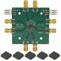
KIT EVAL FOR RF2483
Manufacturer
RFMD
Type
Modulatorr
Datasheet
1.RF2483PCK-410.pdf
(28 pages)
Specifications of RF2483PCK-410
Frequency
700MHz ~ 2.4GHz
For Use With/related Products
RF2483
Lead Free Status / RoHS Status
Lead free / RoHS Compliant
Other names
689-1040
Available stocks
Company
Part Number
Manufacturer
Quantity
Price
Company:

Part Number:
RF2483PCK-410
Manufacturer:
RFMD
Quantity:
5 000


RF2483
The baseband inputs must be driven with balanced differential signals. We suggest amplitude and phase matching <0.5dB
and <0.5°. Phase or gain imbalances between the complementary input signals will cause additional distortion including
some second order baseband distortion.
The common-mode voltage on the baseband inputs should be well controlled at 1.2V. We suggest that the common-mode DC
voltage be 1.2V+0.05V. The common-mode DC voltage is used to bias the modulator; hence, deviations from 1.2V will result
in changes in the current consumption, noise and intermodulation performance.
The chip is designed to be driven with a single-ended LO signal.
The GC DEC and VREF output pins should be decoupled to ground. We recommend a 10nF capacitor on VREF, and a 1nF
capacitor on GC DEC. The purpose of this capacitor is to filter out low frequency noise (20MHz) in the gain control lines, which
may cause noise on the RF signal. The capacitor on the GC DEC line will effect the settling time response to a change in power
control voltage. A 1nF capacitor equates to around a 200ns settling time, and a 0.5nF capacitor equates to a 100ns settling
time. There is a trade-off between settling time and phase noise as you start to apply gain control.
The ground lines for the LO sections, GNDLO and GND1, are brought out of the chip independently from the ground to the RF
and modulator sections. This isolates the LO signals from the RF output sections.
The GND LO pin is effectively the complementary LO input for both the high band and low band LO signals. It has significant
amounts of LO signal flowing through it. This is brought out as an independent ground to try to enable the PCB board designer
to isolate the LO return from the RF output sections and general chip ground.
The RF output ports of the RF2483 consist of open collector architecture and require pull up inductors to the supply voltage.
This, in conjunction with a DC blocking capacitor provides a simple, broadband L-match network as shown in the schematic
diagram. A shunt resistor is included to control the Q of the matching network and set the modulator output power. In this case,
both outputs were designed to provide 0dBm.
An alternate output match containing a third harmonic trap was evaluated. This circuit uses a tapped-C matching network,
whereby the shunt C provides a low impedance path near the third harmonic frequency. Although an additional component is
required, the benefit of suppressing the third harmonic distortion may improve overall system intermodulation. This network
has been shown to provide better than 20dB of improved suppression in high-band mode.
Figure 1. Alternate RF output match with third-harmonic suppression.
12 of 28
7628 Thorndike Road, Greensboro, NC 27409-9421 · For sales or technical
support, contact RFMD at (+1) 336-678-5570 or sales-support@rfmd.com.
2.2 nH
10 nH
L3
L4
180 Ω
130 Ω
R4
R6
Application Notes
VCC
VCC
100 pF
100 pF
2 pF
6 pF
C11
C15
C4
C6
1 pF
2 pF
C12
C13
RFOUT HB
RFOUT LB
J8
J4
Rev A9 DS080403
Related parts for RF2483PCK-410
Image
Part Number
Description
Manufacturer
Datasheet
Request
R

Part Number:
Description:
IC AMP HBT GAAS CATV 8-SOIC
Manufacturer:
RFMD
Datasheet:

Part Number:
Description:
IC AMP MMIC GAAS 12GHZ 4-MICROX
Manufacturer:
RFMD
Datasheet:

Part Number:
Description:
IC AMP 3V LOW-NOISE SOT23-6
Manufacturer:
RFMD
Datasheet:

Part Number:
Description:
KIT EVAL FOR NBB-310
Manufacturer:
RFMD
Datasheet:
Part Number:
Description:
IC AMPLIFIER MMIC LNA 8-QFN
Manufacturer:
RFMD
Datasheet:
Part Number:
Description:
IC AMP MMIC GAAS 4GHZ 4-MICROX
Manufacturer:
RFMD
Datasheet:
Part Number:
Description:
IC SWITCH 10W PHEMT SPDT 12QFN
Manufacturer:
RFMD
Datasheet:
Part Number:
Description:
IC QUADRATURE MODULATOR 16-SOIC
Manufacturer:
RFMD
Datasheet:
Part Number:
Description:
100MHZ TO 4000MHZ, GAAS PHEMT MMIC LOW NOISE AMPLIFIERS
Manufacturer:
RFMD
Part Number:
Description:
KIT EVAL FOR RF2336
Manufacturer:
RFMD
Datasheet:


Part Number:
Description:
IC AMP WLAN/LNA DVR 3V SOT23-5
Manufacturer:
RFMD
Datasheet:

Part Number:
Description:
IC AMP HBT GAAS LNA BYPASS 8-QFN
Manufacturer:
RFMD
Datasheet:

Part Number:
Description:
IC AMP MMIC GAAS 10GHZ 4-MICROX
Manufacturer:
RFMD
Datasheet: