RF2483PCK-410 RFMD, RF2483PCK-410 Datasheet - Page 9
RF2483PCK-410
Manufacturer Part Number
RF2483PCK-410
Description
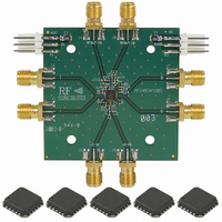
KIT EVAL FOR RF2483
Manufacturer
RFMD
Type
Modulatorr
Datasheet
1.RF2483PCK-410.pdf
(28 pages)
Specifications of RF2483PCK-410
Frequency
700MHz ~ 2.4GHz
For Use With/related Products
RF2483
Lead Free Status / RoHS Status
Lead free / RoHS Compliant
Other names
689-1040
Available stocks
Company
Part Number
Manufacturer
Quantity
Price
Company:

Part Number:
RF2483PCK-410
Manufacturer:
RFMD
Quantity:
5 000


Rev A9 DS080403
Pin
10
11
12
7
8
9
BAND SEL
Function
GND LO
QSIG N
GND1
LOHB
LOLB
Description
Local oscillator input low band.
This input is biased internally at around 1.6V when the chip is in low band
mode and 0V when the chip is in high band mode or powered down. The
LO signal typically needs to be AC coupled.
The noise performance, carrier suppression at low output powers and side-
band suppression are all a function of LO power.
The optimum LO power is between 0dBm and 3dBm.
The device will work with LO powers as low as -20dBm however this is at
the expense of higher noise performance at high output powers and poorer
sideband suppression.
Ground return for the local oscillator input signals.
The GND LO pin is effectively the complementary LO input for both the high
band and low band LO signals. It has significant amounts of LO signal flow-
ing through it. This pin is brought out as an independent ground to enable
the PCB board designer to isolate the LO return from the RF outputs
ground and the general chip ground.
It is recommended that this ground is kept isolated from the die flag
ground. Any connections between the GND LO and any other ground
should be made through a ground plane.
Local oscillator input high band.
This input is biased internally at around 1.6V when the chip is in high band
mode and 0V when the chip is in low band mode or powered down. The LO
HB signal typically needs to be AC coupled.
The noise performance, carrier suppression at low output powers and side-
band suppression are all a function of LO power.
The optimum LO power is between 0dBm and 3dBm.
The device will work with LO powers as low as -20dBm however this is at
the expense of higher noise performance at high output powers and poorer
sideband suppression.
Ground for LO buffers.
Band select input to define active mode.
CMOS input.
Logic 1 (1.4V to VCC)=High band mode.
Logic 2 (0V to 0.5V)=Low band mode.
Quadrature channel negative baseband input port. See QSIGP.
7628 Thorndike Road, Greensboro, NC 27409-9421 · For sales or technical
support, contact RFMD at (+1) 336-678-5570 or sales-support@rfmd.com.
Interface Schematic
See pins 7 and 9.
See pin 6.
V
C C 2
G N D L O
G N D L O
5 0 Ω
V
RF2483
L O L B
L O H B
C C 2
1 2 p F
9 of 28
Related parts for RF2483PCK-410
Image
Part Number
Description
Manufacturer
Datasheet
Request
R

Part Number:
Description:
IC AMP HBT GAAS CATV 8-SOIC
Manufacturer:
RFMD
Datasheet:

Part Number:
Description:
IC AMP MMIC GAAS 12GHZ 4-MICROX
Manufacturer:
RFMD
Datasheet:

Part Number:
Description:
IC AMP 3V LOW-NOISE SOT23-6
Manufacturer:
RFMD
Datasheet:

Part Number:
Description:
KIT EVAL FOR NBB-310
Manufacturer:
RFMD
Datasheet:
Part Number:
Description:
IC AMPLIFIER MMIC LNA 8-QFN
Manufacturer:
RFMD
Datasheet:
Part Number:
Description:
IC AMP MMIC GAAS 4GHZ 4-MICROX
Manufacturer:
RFMD
Datasheet:
Part Number:
Description:
IC SWITCH 10W PHEMT SPDT 12QFN
Manufacturer:
RFMD
Datasheet:
Part Number:
Description:
IC QUADRATURE MODULATOR 16-SOIC
Manufacturer:
RFMD
Datasheet:
Part Number:
Description:
100MHZ TO 4000MHZ, GAAS PHEMT MMIC LOW NOISE AMPLIFIERS
Manufacturer:
RFMD
Part Number:
Description:
KIT EVAL FOR RF2336
Manufacturer:
RFMD
Datasheet:


Part Number:
Description:
IC AMP WLAN/LNA DVR 3V SOT23-5
Manufacturer:
RFMD
Datasheet:

Part Number:
Description:
IC AMP HBT GAAS LNA BYPASS 8-QFN
Manufacturer:
RFMD
Datasheet:

Part Number:
Description:
IC AMP MMIC GAAS 10GHZ 4-MICROX
Manufacturer:
RFMD
Datasheet: