RF3854PCK-410 RFMD, RF3854PCK-410 Datasheet - Page 13
RF3854PCK-410
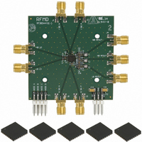
Manufacturer Part Number
RF3854PCK-410
Description
KIT EVAL FOR RF3854
Manufacturer
RFMD
Type
Modulator, PA Driverr
Datasheet
1.RF3854PCK-410.pdf
(26 pages)
Specifications of RF3854PCK-410
Frequency
800MHz ~ 2GHz
For Use With/related Products
RF3854
Lead Free Status / RoHS Status
Lead free / RoHS Compliant
Other names
689-1053
RF3854PCBA
RF3854PCBA


Rev A1 DS070313
Pin
1
2
3
4
5
Function
LO HB P
LO HB N
LO LB N
LO LB P
VCC2
Description
Supply for LO buffers, frequency doubler and dividers.
High band local oscillator input (1800MHz).
In “low band F
quency division of 2 to provide the low band LO signal for the modulator.
In “high band F
high band LO signal for the modulator.
In “high band bypass” a modulated DCS1800/PCS1900 signal (LOHBP-
the signal is routed to the RFOutHb outputs through a differential PA driver
amplifier.
The LOHBP input is AC-coupled internally.
The noise performance, carrier suppression at low output powers and side-
band suppression all vary with LO power. The optimum LO power is
between -3dBm and +3dBm. The device will work with LO powers as low as
-20dBm however this is at the expense of higher phase noise in the LO cir-
cuitry and poorer sideband suppression.
The input impedance should be externally matched to 50Ω. The port can
be driven either differentially or single ended. The port impedance does
not vary significantly between active and power down modes.
The complementary LO input for both LOHBP LO signals.
In any of the modes the LOHB input may be driven either single ended or
differentially. If the LO is driven single ended then the PCB board designer
can ground this pin.
It is recommended that if this pin is grounded that it is kept isolated from
the GND1 pin and the die flag ground. All connections to any other ground
should be made through a ground plane. Poor routing of this ground signal
can significantly degrade the LO leakage performance.
Low band local oscillator input (900MHz).
In “wideband F
In “Low band F
signal for the modulator.
In “Low band Bypass” a modulated GSM900 signal (LOLBP-LOLBN) is
switched into the RF signal path. The modulator is disabled and the signal
is routed to the RFOutLb outputs through a differential PA driver amplifier.
This LOLBP input is AC-coupled internally.
The noise performance, carrier suppression at low output powers and side-
band suppression performance are functions of LO power. The optimum LO
power is between -3dBm and +3dBm. The device will work with LO powers
as low as -20dBm however this is at the expense of higher noise perfor-
mance at high output powers and poorer sideband suppression.
The input impedance should be externally matched to 50Ω. The port
impedance does not vary significantly between active and powered modes.
The complementary LO input for both LOLBP LO signals.
In any of the modes the LOLB input may be driven either single ended or
differentially. If the LO is driven single ended then the PCB board designer
can ground this pin.
It is recommended that if this pin is grounded that it is kept isolated from
the GND1 pin and the die flag ground. All connections to any other ground
should be made through a ground plane. Poor routing of this GndLO signal
can significantly degrade the LO leakage performance.
LOHBN) is switched into the RF signal path. The modulator is disabled and
LOLBN) is doubled in frequency to provide the LO signal for the modulator.
7628 Thorndike Road, Greensboro, NC 27409-9421 · For sales or technical
support, contact RFMD at (+1) 336-678-5570 or sales-support@rfmd.com.
LO
LO
LO
LO
/2” modes the signal (LOHBP-LOHBN) undergoes a fre-
x2” and “high band F
x1” modes the signal (LOLBP-LOLBN) is used as the LO
x1” modes the signal (LOHBP-LOHBN) is used as the
LO
x2” modes the signal (LOLBP-
LO LB P
LO LB N
Interface Schematic
LO HB N
See pin 2.
See pin 4.
LO HB P
Modulator and
VCC2
VGA
V
RF3854
V
CC
CC
13 of 26
Related parts for RF3854PCK-410
Image
Part Number
Description
Manufacturer
Datasheet
Request
R

Part Number:
Description:
IC AMP HBT GAAS CATV 8-SOIC
Manufacturer:
RFMD
Datasheet:

Part Number:
Description:
IC AMP MMIC GAAS 12GHZ 4-MICROX
Manufacturer:
RFMD
Datasheet:

Part Number:
Description:
IC AMP 3V LOW-NOISE SOT23-6
Manufacturer:
RFMD
Datasheet:

Part Number:
Description:
KIT EVAL FOR NBB-310
Manufacturer:
RFMD
Datasheet:
Part Number:
Description:
IC AMPLIFIER MMIC LNA 8-QFN
Manufacturer:
RFMD
Datasheet:
Part Number:
Description:
IC AMP MMIC GAAS 4GHZ 4-MICROX
Manufacturer:
RFMD
Datasheet:
Part Number:
Description:
IC SWITCH 10W PHEMT SPDT 12QFN
Manufacturer:
RFMD
Datasheet:
Part Number:
Description:
IC QUADRATURE MODULATOR 16-SOIC
Manufacturer:
RFMD
Datasheet:
Part Number:
Description:
100MHZ TO 4000MHZ, GAAS PHEMT MMIC LOW NOISE AMPLIFIERS
Manufacturer:
RFMD
Part Number:
Description:
KIT EVAL FOR RF2336
Manufacturer:
RFMD
Datasheet:


Part Number:
Description:
IC AMP WLAN/LNA DVR 3V SOT23-5
Manufacturer:
RFMD
Datasheet:

Part Number:
Description:
IC AMP HBT GAAS LNA BYPASS 8-QFN
Manufacturer:
RFMD
Datasheet:

Part Number:
Description:
IC AMP MMIC GAAS 10GHZ 4-MICROX
Manufacturer:
RFMD
Datasheet: