RF3854PCK-410 RFMD, RF3854PCK-410 Datasheet - Page 16
RF3854PCK-410
Manufacturer Part Number
RF3854PCK-410
Description
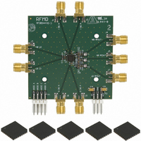
KIT EVAL FOR RF3854
Manufacturer
RFMD
Type
Modulator, PA Driverr
Datasheet
1.RF3854PCK-410.pdf
(26 pages)
Specifications of RF3854PCK-410
Frequency
800MHz ~ 2GHz
For Use With/related Products
RF3854
Lead Free Status / RoHS Status
Lead free / RoHS Compliant
Other names
689-1053
RF3854PCBA
RF3854PCBA


RF3854
16 of 26
Base
Pkg
Pin
20
22
23
21
24
DIE FLAG
Function
MODE A
MODE B
I SIG P
I SIG N
VCC1
Description
Mode control pin. See the Logic Truth table.
CMOS Logic inputs: Logic 0=0V to 0.4V; Logic 1=1.4V to V
Supply for modulator, VGA and PA driver amplifiers.
In-phase I channel positive baseband input port.
Best performance is achieved when the ISIGP and ISIGN are driven differ-
entially with a 1.2V common mode DC voltage. The recommended differ-
ential drive level (V
modulation and 1.0V
This input should be DC-biased at 1.2V. In sleep mode an internal FET
switch is opened, the input goes high impedance and the modulator is de-
biased.
Phase or amplitude errors between the ISIGP and ISIGN signals will result
in a common-mode signal which may result in an increase in the even
order distortion of the modulation in the output spectrum.
DC offsets between the ISIGP and ISIGN signals will result in increased
carrier leakage. Small DC offsets may be deliberately applied between the
ISIGP/ISIGN and QSIGP/QSIGN inputs to cancel out the LO leakage. The
optimum corrective DC offsets will change with mode, frequency and gain
control.
Common-mode noise on the ISIGP and ISIGN should be kept low as it may
degrade the noise performance of the modulator.
Phase offsets from quadrature between the I and Q baseband signals
results in degrades sideband suppression.
In-phase I channel negative baseband input port. See pin 22.
Mode control pin. See the Logic Truth table.
CMOS Logic inputs: Logic 0=0V to 0.4V; Logic 1=1.4V to V
Ground for LO section, modular, biasing, variable gain amplifier, and sub-
strate.
7628 Thorndike Road, Greensboro, NC 27409-9421 · For sales or technical
support, contact RFMD at (+1) 336-678-5570 or sales-support@rfmd.com.
ISIGP
P-P
-V
for GMSK modulation.
ISIGN
) is 1.2V
P-P
for EDGE, 0.8V
P-P
CC
CC
W-CDMA
.
.
Interface Schematic
See pin 6.
See pin 22.
See pin 6.
LO Quadrature
Generator and
VCC1
GND1
V
CC2
Buffers
x1
Rev A1 DS070313
Related parts for RF3854PCK-410
Image
Part Number
Description
Manufacturer
Datasheet
Request
R

Part Number:
Description:
IC AMP HBT GAAS CATV 8-SOIC
Manufacturer:
RFMD
Datasheet:

Part Number:
Description:
IC AMP MMIC GAAS 12GHZ 4-MICROX
Manufacturer:
RFMD
Datasheet:

Part Number:
Description:
IC AMP 3V LOW-NOISE SOT23-6
Manufacturer:
RFMD
Datasheet:

Part Number:
Description:
KIT EVAL FOR NBB-310
Manufacturer:
RFMD
Datasheet:
Part Number:
Description:
IC AMPLIFIER MMIC LNA 8-QFN
Manufacturer:
RFMD
Datasheet:
Part Number:
Description:
IC AMP MMIC GAAS 4GHZ 4-MICROX
Manufacturer:
RFMD
Datasheet:
Part Number:
Description:
IC SWITCH 10W PHEMT SPDT 12QFN
Manufacturer:
RFMD
Datasheet:
Part Number:
Description:
IC QUADRATURE MODULATOR 16-SOIC
Manufacturer:
RFMD
Datasheet:
Part Number:
Description:
100MHZ TO 4000MHZ, GAAS PHEMT MMIC LOW NOISE AMPLIFIERS
Manufacturer:
RFMD
Part Number:
Description:
KIT EVAL FOR RF2336
Manufacturer:
RFMD
Datasheet:


Part Number:
Description:
IC AMP WLAN/LNA DVR 3V SOT23-5
Manufacturer:
RFMD
Datasheet:

Part Number:
Description:
IC AMP HBT GAAS LNA BYPASS 8-QFN
Manufacturer:
RFMD
Datasheet:

Part Number:
Description:
IC AMP MMIC GAAS 10GHZ 4-MICROX
Manufacturer:
RFMD
Datasheet: