1321XDSK-BDM Freescale Semiconductor, 1321XDSK-BDM Datasheet - Page 24
1321XDSK-BDM
Manufacturer Part Number
1321XDSK-BDM
Description
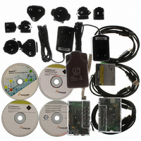
KIT STARTER DEV 1321X W/USB
Manufacturer
Freescale Semiconductor
Type
Sensor Demor
Specifications of 1321XDSK-BDM
Frequency
2.4GHz
Wireless Frequency
2.4 GHz
Interface Type
SPI
Modulation
DSSS OQPSK
Security
128 bit AES
Operating Voltage
2 VDC to 3.4 VDC
Output Power
2 dBm
Antenna
F-Antenna
Operating Temperature Range
- 40 C to + 85 C
For Use With/related Products
MC1321x
Lead Free Status / RoHS Status
Contains lead / RoHS compliant by exemption


24
3.
Balun
required by the radio. Separate RFIN and PAO signals are provided for connection with the baluns,
and the CT_Bias signal is programmed to provide the external switch control. The polarity of the
external switch control is selectable.
Figure 14C
the receive side, the RX antenna is ac-coupled to the differential RFIN inputs and these capacitors
along with inductor L1 form a matching network. Inductors L2 and L3 are ac-coupled to ground to
form a frequency trap. For the transmit side, the TX antenna is connected to the differential PAO
outputs, and inductors L4 and L5 provide dc-biasing to VDDA but are ac isolated.
14A) Using Onboard T/R Switch
Bypass
shows a dual antenna configuration where there is a RX antenna and a TX antenna. For
L1
Figure 14. Using the MC1321x with External RF Components
PAO_M
RFIN_M (PAO_M)
PAO_P
RFIN_P (PAO_P)
CT_Bias
RX Antenna
TX Antenna
L1
MC1321x
MC13211/212/213 Technical Data, Rev. 1.8
Bypass
L2
L4
14C) Using Dual Antennae
VDDA
L3
L5
Bypass
A nt
S w
14B) Using External Antenna Switch With LNA
RFIN_P (PAO_P)
PAO_M
RFIN_M (PAO_M)
CT_Bias
PAO_P
V D D
L NA
MC1321x
B a lun
B a lun
B yp a ss
B yp a s s
V D D A
Freescale Semiconductor
L 1
R F IN _ M (P A O _ M )
P A O _ M
P A O _ P
RF IN_ P (P A O _ P )
(A nt S w C tl)
C T_ B ia s
M C 1321x
Related parts for 1321XDSK-BDM
Image
Part Number
Description
Manufacturer
Datasheet
Request
R

Part Number:
Description:
KIT STARTER DEVELOPER 1321X
Manufacturer:
Freescale Semiconductor
Datasheet:

Part Number:
Description:
Manufacturer:
Freescale Semiconductor, Inc
Datasheet:
Part Number:
Description:
Manufacturer:
Freescale Semiconductor, Inc
Datasheet:
Part Number:
Description:
Manufacturer:
Freescale Semiconductor, Inc
Datasheet:
Part Number:
Description:
Manufacturer:
Freescale Semiconductor, Inc
Datasheet:
Part Number:
Description:
Manufacturer:
Freescale Semiconductor, Inc
Datasheet:
Part Number:
Description:
Manufacturer:
Freescale Semiconductor, Inc
Datasheet:
Part Number:
Description:
Manufacturer:
Freescale Semiconductor, Inc
Datasheet:
Part Number:
Description:
Manufacturer:
Freescale Semiconductor, Inc
Datasheet:
Part Number:
Description:
Manufacturer:
Freescale Semiconductor, Inc
Datasheet:
Part Number:
Description:
Manufacturer:
Freescale Semiconductor, Inc
Datasheet:
Part Number:
Description:
Manufacturer:
Freescale Semiconductor, Inc
Datasheet:
Part Number:
Description:
Manufacturer:
Freescale Semiconductor, Inc
Datasheet:
Part Number:
Description:
Manufacturer:
Freescale Semiconductor, Inc
Datasheet:
Part Number:
Description:
Manufacturer:
Freescale Semiconductor, Inc
Datasheet: