AD6655-125EBZ Analog Devices Inc, AD6655-125EBZ Datasheet - Page 49
AD6655-125EBZ
Manufacturer Part Number
AD6655-125EBZ
Description
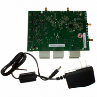
BOARD EVAL W/AD6655 & SOFTWARE
Manufacturer
Analog Devices Inc
Type
Receiver, CDMAr
Specifications of AD6655-125EBZ
Frequency
450MHz
Silicon Manufacturer
Analog Devices
Application Sub Type
IF Diversity Receiver
Kit Application Type
Communication & Networking
Silicon Core Number
AD6655
Kit Contents
Evaluation Board With AD6655 And Software
Lead Free Status / RoHS Status
Lead free / RoHS Compliant
For Use With/related Products
AD6655
Lead Free Status / Rohs Status
Compliant


CONFIGURATION WITHOUT THE SPI
In applications that do not interface to the SPI control registers,
the SDIO/DCS pin, the SCLK/DFS pin, the SMI SDO/OEB pin,
and the SMI SCLK/PDWN pin serve as standalone CMOS-
compatible control pins. When the device is powered up, it is
assumed that the user intends to use the pins as static control
lines for the duty cycle stabilizer, output data format, output
enable, and power-down feature control. In this mode, the CSB
chip select should be connected to AVDD, which disables the
serial port interface.
Table 27. Mode Selection
Pin
SDIO/DCS
SCLK/DFS
SMI SDO/OEB
SMI SCLK/PDWN
SCLK
SDIO
CSB
DON’T CARE
DON’T CARE
t
S
R/W
External
Voltage
AVDD (default)
AGND
AVDD
AGND (default)
AVDD
AGND (default)
AVDD
AGND (default)
t
DS
W1
W0
t
DH
A12
Configuration
Duty cycle stabilizer
enabled
Duty cycle stabilizer
disabled
Twos complement
enabled
Offset binary enabled
Outputs in high
impedance
Outputs enabled
Chip in power-down or
standby
Normal operation
t
HIGH
A11
t
Figure 81. Serial Port Interface Timing Diagram
LOW
A10
A9
Rev. A | Page 49 of 88
t
CLK
A8
A7
SPI ACCESSIBLE FEATURES
Table 28 provides a brief description of the general features that
are accessible via the SPI. These features are described in detail
in Application Note AN-877, Interfacing to High Speed ADCs via
SPI (see www.analog.com). The AD6655 part-specific features
are described in the Memory Map Register Description section.
Table 28. Features Accessible Using the SPI
Feature Name
Mode
Clock
Offset
Test I/O
Output Mode
Output Phase
Output Delay
VREF
D5
D4
Description
Allows the user to set either power-down mode
or standby mode
Allows the user to access the DCS via the SPI
Allows the user to digitally adjust the
converter offset
Allows the user to set test modes to have
known data on output bits
Allows the user to set up outputs
Allows the user to set the output clock polarity
Allows the user to vary the DCO delay
Allows the user to set the reference voltage
D3
D2
D1
D0
t
H
DON’T CARE
AD6655
DON’T CARE
Related parts for AD6655-125EBZ
Image
Part Number
Description
Manufacturer
Datasheet
Request
R

Part Number:
Description:
BOARD EVAL FOR 150MSPS AD6655
Manufacturer:
Analog Devices Inc
Datasheet:

Part Number:
Description:
±1.7g Dual-Axis IMEMS Accelerometer Evaluation Board
Manufacturer:
Analog Devices Inc
Datasheet:

Part Number:
Description:
Inertial Sensor Evaluation System
Manufacturer:
Analog Devices Inc
Datasheet:
Part Number:
Description:
Manufacturer:
Analog Devices Inc
Datasheet:
Part Number:
Description:
Manufacturer:
Analog Devices Inc
Datasheet:
Part Number:
Description:
Manufacturer:
Analog Devices Inc
Datasheet:
Part Number:
Description:
Manufacturer:
Analog Devices Inc
Datasheet:
Part Number:
Description:
Manufacturer:
Analog Devices Inc
Datasheet:
Part Number:
Description:
Manufacturer:
Analog Devices Inc
Datasheet:
Part Number:
Description:
Manufacturer:
Analog Devices Inc
Datasheet:
Part Number:
Description:
Manufacturer:
Analog Devices Inc
Datasheet:
Part Number:
Description:
Manufacturer:
Analog Devices Inc
Datasheet:
Part Number:
Description:
Manufacturer:
Analog Devices Inc
Datasheet: