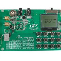
SI4735-B-EVB Silicon Laboratories Inc, SI4735-B-EVB Datasheet
SI4735-B-EVB
Specifications of SI4735-B-EVB


Related parts for SI4735-B-EVB


SI4735-B-EVB Summary of contents
Page 1
... EN55020 complaint Programmable reference clock Digital volume control Adjustable soft mute control RDS/RBDS processor (Si4735 only) Optional digital audio out (Si4735 only) 2-wire and 3-wire control interface 2.7 to 5.5 V supply voltage Wide range of ferrite loop sticks and air loop antennas supported ...
Page 2
Si4734/35-B20 2 Rev. 1.0 ...
Page 3
... LW Receiver . . . . . . . . . . . . . . . . . . . . . . . . . . . . . . . . . . . . . . . . . . . . . . . . . . . . . . .20 4.7. Digital Audio Interface (Si4735 Only 4.8. Stereo Audio Processing . . . . . . . . . . . . . . . . . . . . . . . . . . . . . . . . . . . . . . . . . . . . . . 23 4.9. De-emphasis . . . . . . . . . . . . . . . . . . . . . . . . . . . . . . . . . . . . . . . . . . . . . . . . . . . . . . . 23 4.10. Stereo DAC . . . . . . . . . . . . . . . . . . . . . . . . . . . . . . . . . . . . . . . . . . . . . . . . . . . . . . . 23 4.11. Soft Mute . . . . . . . . . . . . . . . . . . . . . . . . . . . . . . . . . . . . . . . . . . . . . . . . . . . . . . . . . 23 4.12. RDS/RBDS Processor (Si4735 Only .23 4.13. Tuning . . . . . . . . . . . . . . . . . . . . . . . . . . . . . . . . . . . . . . . . . . . . . . . . . . . . . . . . . . . 24 4.14. Seek . . . . . . . . . . . . . . . . . . . . . . . . . . . . . . . . . . . . . . . . . . . . . . . . . . . . . . . . . . . . 24 4.15. Reference Clock . . . . . . . . . . . . . . . . . . . . . . . . . . . . . . . . . . . . . . . . . . . . . . . . . . . 24 4.16. Control Interface . . . . . . . . . . . . . . . . . . . . . . . . . . . . . . . . . . . . . . . . . . . . . . . . . . . 24 4.17. GPO Outputs . . . . . . . . . . . . . . . . . . . . . . . . . . . . . . . . . . . . . . . . . . . . . . . . . . . . . . 26 4.18. Firmware Upgrades . . . . . . . . . . . . . . . . . . . . . . . . . . . . . . . . . . . . . . . . . . . . . . . . .26 4 ...
Page 4
Si4734/35-B20 1. Electrical Specifications Table 1. Recommended Operating Conditions Parameter Supply Voltage Interface Supply Voltage Power Supply Powerup Rise Time Interface Power Supply Powerup Rise Time Ambient Temperature Note: All minimum and maximum specifications are guaranteed and apply across the ...
Page 5
Table 3. DC Characteristics (V = 2 1 Parameter FM Mode Supply Current 1 Supply Current 2 RDS Supply Current 2 Supply Current AM/SW/LW Mode Supply Current 2 Supply ...
Page 6
Si4734/35-B20 Table 4. Reset Timing Characteristics (V = 2 1 Parameter RST Pulse Width and GPO1, GPO2/INT Setup to RST↑ GPO1, GPO2/INT Hold from RST↑ Important Notes: 1. When ...
Page 7
Table 5. 2-Wire Control Interface Characteristics (V = 2 1 Parameter SCLK Frequency SCLK Low Time SCLK High Time ↓ SCLK Input to SDIO Setup (START) ↓ SCLK Input ...
Page 8
Si4734/35-B20 SU:STA HD:STA LOW 70% SCLK 30% 70% SDIO 30% START t r:IN Figure 2. 2-Wire Control Interface Read and Write Timing Parameters SCLK A6-A0, SDIO R/W START ADDRESS + R/W Figure 3. 2-Wire Control Interface Read ...
Page 9
Table 6. 3-Wire Control Interface Characteristics (V = 2 1 Parameter SCLK Frequency SCLK High Time SCLK Low Time SDIO Input, SEN to SCLK↑ Setup SDIO Input to SCLK↑ ...
Page 10
Si4734/35-B20 Table 7. SPI Control Interface Characteristics (V = 2 1 Parameter SCLK Frequency SCLK High Time SCLK Low Time SDIO Input, SEN to SCLK↑ Setup SDIO Input to ...
Page 11
Table 8. Digital Audio Interface Characteristics (V = 2 1 Parameter DCLK Cycle Time DCLK Pulse Width High DCLK Pulse Width Low DFS Set-up Time to DCLK Rising Edge ...
Page 12
Si4734/35-B20 Table 9. FM Receiver Characteristics (V = 2 1 Parameter Input Frequency Sensitivity with Headphone 3,4,5 Network Sensitivity with 50 Ω Network 3,4,5,6 6 RDS Sensitivity 6,7 LNA ...
Page 13
Table 9. FM Receiver Characteristics (V = 2 1 Parameter 6 Seek/Tune Time 6 Powerup Time 12 RSSI Offset Notes: 1. Additional testing information is available in Application Note ...
Page 14
Si4734/35-B20 Table 10. 64–75.9 MHz Input Frequency FM Receiver Characteristics (V = 2 1 Parameter Input Frequency Sensitivity with Headphone 2,3,4,5 Network 5,6 LNA Input Resistance 5,6 LNA Input ...
Page 15
Table 11. AM/SW/LW Receiver Characteristics (V = 2 1 – ° Parameter Symbol Input Frequency 2,3,4,5, 6 Sensitivity 5,7 Large Signal Voltage Handling Power Supply Rejection ...
Page 16
Si4734/35-B20 Table 12. Reference Clock and Crystal Characteristics (V = 2 1 Parameter * RCLK Supported Frequencies RCLK Frequency Tolerance REFCLK_PRESCALE REFCLK Crystal Oscillator Frequency Crystal Frequency Tolerance* Board ...
Page 17
Typical Application Schematic FMI FMI C4 3 RFGND AMI C5 5 RST RST SEN SCLK SDIO RCLK VIO 1.5 to 3.6 V Notes: 1. Place C1 close to V pin All ...
Page 18
Si4734/35-B20 3. Bill of Materials Component(s) C1 Supply bypass capacitor, 22 nF, ±20%, Z5U/X7R C4 Capacitor, 18 pF, ±20%, Z5U/X7R C5 Coupling capacitor, 0.47 µF, ±20%, Z5U/X7R L1 Ferrite loop stick, 180 L2 4.7 µH U1 Si4734/35 AM/FM Radio Tuner ...
Page 19
... The Si4735 incorporates a digital processor for the European Radio Data System (RDS) and the North American Radio Broadcast Data System (RBDS), including all synchronization, error detection, and error correction functions ...
Page 20
... AMI (pin 4) and processed by the AM front-end circuitry. In addition to the receiver mode, a clocking mode allows the Si4734/ clocked from a reference clock or crystal. On the Si4735, an audio output mode is available as analog and/or digital audio output. In the analog audio output mode, pin 13 is ROUT, pin 14 is LOUT, pin 17 is GPO3 ...
Page 21
... Digital Audio Interface (Si4735 Only) The digital audio interface operates in slave mode and supports three different audio data formats Left-Justified DSP Mode 4.7.1. Audio Data Formats mode, by default the MSB is captured on the second rising edge of DCLK following each DFS transition. The remaining bits of the word are sent in order, down to the LSB ...
Page 22
Si4734/35-B20 INVERTED (OFALL = 1) DCLK (OFALL = 0) DCLK DFS (OMODE = 0000) 1 DCLK DOUT 1 2 MSB INVERTED (OFALL = 1) DCLK (OFALL = 0) DCLK DFS Left-Justified (OMODE = 0110) DOUT 1 2 ...
Page 23
... The Si4735 implements an RDS/RBDS* processor for symbol decoding, detection, and error correction. The Si4735 device is user configurable and provides an optional interrupt when RDS is synchronized, loses synchronization, and/or the user configurable RDS FIFO threshold has been met. The Si4735 reports RDS decoder synchronization status, and detailed bit errors in the information word for each RDS block with the FM_RDS_STATUS command ...
Page 24
Si4734/35-B20 4.13. Tuning The frequency synthesizer uses Silicon Laboratories’ proven technology, including a completely integrated VCO. The frequency synthesizer quadrature local oscillator signal used to downconvert the RF input to a low intermediate frequency. The VCO frequency is locked to ...
Page 25
SDIO low on the next falling edge of SCLK. Although the Si4734/35 will respond to only a single device address, this address can be changed with the SEN pin (note that the SEN pin is not used ...
Page 26
... GPO2/INT can be configured to provide interrupts and GPO3 can be configured to provide external crystal support or as DCLK in digital audio output mode. In digital output mode (Si4735 only), GPO6 and GPO7 can be configured as DFS and DOUT respectively. 4.18. Firmware Upgrades The Si4734/35 contains on-chip program RAM to accommodate minor changes to the firmware ...
Page 27
... Queries the status of the Received Signal Quality (RSQ) of the current chan- nel (Si4735 only). Returns RDS information for current channel and reads an entry from the RDS FIFO (Si4735 only). Tunes to a given AM or SW/LW frequency. Begins searching for a valid AM or SW/LW frequency depending on the AM_SEEK_BAND_BOTTOM and AM_SEEK_BAND_TOP settings ...
Page 28
... Description Enables interrupt sources. Configures the digital output sample rate in 100 Hz steps. The digital output sample rate is disabled by default (Si4735 only). Sets frequency of reference clock in Hz. The range is 31130 to 34406 Hz disable the AFC. Default is 32768 Hz. Sets the prescaler value for RCLK input. ...
Page 29
Table 15. Si473x Property Summary (Continued) Prop Name 0x1502 RDS_CONFIG 0x3100 AM_DEEMPHASIS 0x3102 AM_CHANNEL_FILTER 0x3200 AM_RSQ_INTERRUPTS AM_RSQ_SNR_HIGH_ 0x3201 THRESHOLD AM_RSQ_SNR_LOW_ 0x3202 THRESHOLD AM_RSQ_RSSI_HIGH_ 0x3203 THRESHOLD AM_RSQ_RSSI_LOW_ 0x3204 THRESHOLD 0x3300 AM_SOFT_MUTE_RATE 0x3301 AM_SOFT_MUTE_SLOPE AM_SOFT_MUTE_MAX_ 0x3302 ATTENUATION AM_SOFT_MUTE_SNR_ 0x3303 THRESHOLD AM_SEEK_BAND_ 0x3400 ...
Page 30
Si4734/35-B20 6. Pin Descriptions: Si4734/35-GM RFGND Pin Number(s) Name connect. Leave floating. 2 FMI FM RF inputs. 3 RFGND RF ground. Connect to ground plane on PCB. 4 AMI AM/SW/LW RF input. 5 RST Device reset ...
Page 31
... Ordering Guide Part Number* Si4734-B20-GM AM/FM/SW/LW Broadcast Radio Receiver Si4735-B20-GM AM/FM/SW/LW Broadcast Radio Receiver with RDS/RBDS *Note: Add an “(R)” at the end of the device part number to denote tape and reel option; 2500 quantity per reel. Description Rev. 1.0 Si4734/35-B20 Package Operating ...
Page 32
... Line 3 Marking: Circle = 0.5 mm Diameter (Bottom-Left Justified Year WW = Workweek 32 3520 BTTT YWW 34 = Si4734 Si4735 20 = Firmware Revision 2 Revision B Die Internal tracking code. Pin 1 Identifier Assigned by the Assembly House. Corresponds to the last sig- nificant digit of the year and workweek of the mold date. Rev. 1.0 ...
Page 33
Package Outline: Si4734/35 QFN Figure 14 illustrates the package details for the Si4734/35. Table 16 lists the values for the dimensions shown in the illustration. Figure 14. 20-Pin Quad Flat No-Lead (QFN) Symbol Millimeters Min Nom A 0.50 0.55 ...
Page 34
Si4734/35-B20 10. PCB Land Pattern: Si4734/35 QFN Figure 15 illustrates the PCB land pattern details for the Si4734/35-GM. Table 17 lists the values for the dimensions shown in the illustration. 34 Figure 15. PCB Land Pattern Rev. 1.0 ...
Page 35
Table 17. PCB Land Pattern Dimensions Symbol Millimeters Min Max D 2.71 REF D2 1.60 1.80 e 0.50 BSC E 2.71 REF E2 1.60 1.80 f 2.53 BSC GD 2.10 — Notes: General 1. All dimensions shown are in millimeters ...
Page 36
Si4734/35-B20 11. Additional Reference Resources EN55020 Compliance Test Certificate AN231: Si4700/01 Headphone and Antenna Interface AN332: Universal Programming Guide AN383: Antenna Selection and Universal Layout Guidelines AN386: Si473x Ferrite Loop Stick Antenna Interface AN388: Universal Evaluation Board Test Procedure AN389: ...
Page 37
OCUMENT HANGE IST Revision 0.4 to Revision 1.0 Updated Table 1, “Recommended Operating Conditions,” on page 4. Updated Table 3, “DC Characteristics,” on page 5. Updated Table 5, “2-Wire Control Interface 1,2,3 Characteristics ,” on page 7. ...
Page 38
... Should Buyer purchase or use Silicon Laboratories products for any such unintended or unauthorized ap- plication, Buyer shall indemnify and hold Silicon Laboratories harmless against all claims and damages. Silicon Laboratories and Silicon Labs are trademarks of Silicon Laboratories Inc. Other products or brandnames mentioned herein are trademarks or registered trademarks of their respective holders. ...