SI4735-B-EVB Silicon Laboratories Inc, SI4735-B-EVB Datasheet - Page 24
SI4735-B-EVB
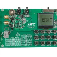
Manufacturer Part Number
SI4735-B-EVB
Description
BOARD EVAL SI4735 VERSION B
Manufacturer
Silicon Laboratories Inc
Type
Receiverr
Specifications of SI4735-B-EVB
Frequency
153kHz ~ 279kHz, 520kHz ~ 1.71GHz, 2.3MHz ~ 21.85MHz, 76MHz ~ 108MHz
Lead Free Status / RoHS Status
Lead free / RoHS Compliant
For Use With/related Products
SI4735
Lead Free Status / RoHS Status
Lead free / RoHS Compliant, Lead free / RoHS Compliant


Si4734/35-B20
4.13. Tuning
The frequency synthesizer uses Silicon Laboratories’
proven technology, including a completely integrated
VCO.
quadrature local oscillator signal used to downconvert
the RF input to a low intermediate frequency. The VCO
frequency is locked to the reference clock and adjusted
with an automatic frequency control (AFC) servo loop
during reception. The tuning frequency can be directly
programmed
AM_TUNE_FREQ commands. The Si4734/35 supports
channel spacing steps of 10 kHz in FM mode and 1 kHz
in AM/SW/LW mode.
4.14. Seek
Seek tuning will search up or down for a valid channel.
Valid channels are found when the receive signal
strength indicator (RSSI) and the signal-to-noise ratio
(SNR) values exceed the set threshold. Using the SNR
qualifier rather than solely relying on the more
traditional RSSI qualifier can reduce false stops and
increase the number of valid stations detected. Seek is
initiated
AM_SEEK_START commands. The RSSI and SNR
threshold settings are adjustable using properties (see
Table 15).
Two seek options are available. The device will either
wrap or stop at the band limits. If the seek operation is
unable to find a channel, the device will indicate failure
and return to the channel selected before the seek
operation began.
4.15. Reference Clock
The Si4734/35 reference clock is programmable,
supporting RCLK frequencies in Table 12. Refer to
Table 3, “DC Characteristics,” on page 5 for switching
voltage
Characteristics” on page 12 for frequency tolerance
information.
An onboard crystal oscillator is available to generate the
32.768 kHz reference when an external crystal and load
capacitors are provided. Refer to "2. Typical Application
Schematic" on page 17. This mode is enabled using the
POWER_UP
Command Summary,” on page 27.
The Si4734/35 performance may be affected by data
activity on the SDIO bus when using the integrated
internal oscillator. SDIO activity results from polling the
tuner for status or communicating with other devices
that share the SDIO bus. If there is SDIO bus activity
while the Si4734/35 is performing the seek/tune
function, the crystal oscillator may experience jitter,
which may result in mistunes, false stops, and/or lower
SNR.
24
The
levels
using
frequency
command,
using
and
the
the
synthesizer
Table 9,
FM_SEEK_START
see
FM_TUNE_FREQ
Table 14,
“FM
generates
Receiver
“Si473x
and
and
the
Rev. 1.0
For
recommends that all SDIO data traffic be suspended
during Si4734/35 seek and tune operations. This is
achieved by keeping the bus quiet for all other devices
on the bus, and delaying tuner polling until the tune or
seek operation is complete. The seek/tune complete
(STC) interrupt should be used instead of polling to
determine when a seek/tune operation is complete.
4.16. Control Interface
A serial port slave interface is provided, which allows an
external controller to send commands to the Si4734/35
and receive responses from the device. The serial port
can operate in three bus modes: 2-wire mode, 3-wire
mode, or SPI mode. The Si4734/35 selects the bus
mode by sampling the state of the GPO1 and GPO2
pins on the rising edge of RST. The GPO1 pin includes
an internal pull-up resistor, which is connected while
RST is low, and the GPO2 pin includes an internal pull-
down resistor, which is connected while RST is low.
Therefore, it is only necessary for the user to actively
drive pins which differ from these states. See Table 13.
After the rising edge of RST, the pins GPO1 and GPO2
are used as general purpose output (O) pins, as
described in Section “4.17. GPO Outputs”. In any bus
mode, commands may only be sent after V
supplies are applied.
In any bus mode, before sending a command or reading
a response, the user must first read the status byte to
ensure that the device is ready (CTS bit is high).
4.16.1. 2-Wire Control Interface Mode
When selecting 2-wire mode, the user must ensure that
SCLK is high during the rising edge of RST, and stays
high until after the first start condition. Also, a start
condition must not occur within 300 ns before the rising
edge of RST.
The 2-wire bus mode uses only the SCLK and SDIO
pins for signaling. A transaction begins with the START
condition, which occurs when SDIO falls while SCLK is
high. Next, the user drives an 8-bit control word serially
on SDIO, which is captured by the device on rising
edges of SCLK. The control word consists of a 7-bit
device address, followed by a read/write bit (read = 1,
write = 0). The Si4734/35 acknowledges the control
Table 13. Bus Mode Select on Rising Edge of
Bus Mode
best
2-Wire
3-Wire
SPI
seek/tune
0 (must drive)
results, Silicon
GPO1
RST
1
1
1 (must drive)
Laboratories
GPO2
IO
0
0
and V
DD
Related parts for SI4735-B-EVB
Image
Part Number
Description
Manufacturer
Datasheet
Request
R

Part Number:
Description:
BOARD EVAL SI4735 VERSION C
Manufacturer:
Silicon Laboratories Inc
Datasheet:
Part Number:
Description:
IC RX AM/FM/SW/LW RAD RDS 20UQFN
Manufacturer:
Silicon Laboratories Inc
Datasheet:
Part Number:
Description:
IC RX AM/FM/SW/LW RAD RDS 20UQFN
Manufacturer:
Silicon Laboratories Inc
Datasheet:
Part Number:
Description:
IC RX AM/FM/SW/LW RAD RDS 20UQFN
Manufacturer:
Silicon Laboratories Inc
Datasheet:
Part Number:
Description:
IC RX AM/FM/SW/LW RAD RDS 24SSOP
Manufacturer:
Silicon Laboratories Inc
Datasheet:

Part Number:
Description:
IC RX AM/FM/SW/LW RAD RDS 20UQFN
Manufacturer:
Silicon Laboratories Inc
Datasheet:
Part Number:
Description:
BOARD EVALUATION FOR SI4734/35
Manufacturer:
Silicon Laboratories Inc
Datasheet:
Part Number:
Description:
RF RX FM AM SW LW 24 SSOP
Manufacturer:
Silicon Laboratories Inc
Datasheet:
Part Number:
Description:
IC RAD RX AM/FM/SW/LW/AUX 20QFN
Manufacturer:
Silicon Laboratories Inc
Datasheet:
Part Number:
Description:
IC RX AM/FM/SW/LW RAD RDS 24SSOP
Manufacturer:
Silicon Laboratories Inc
Datasheet:
Part Number:
Description:
RECEIVER, RADIO, MULTIBAND, 20QFN
Manufacturer:
Silicon Laboratories Inc
Datasheet:
Part Number:
Description:
SMD/C�/SINGLE-ENDED OUTPUT SILICON OSCILLATOR
Manufacturer:
Silicon Laboratories Inc
Part Number:
Description:
Manufacturer:
Silicon Laboratories Inc
Datasheet:
Part Number:
Description:
N/A N/A/SI4010 AES KEYFOB DEMO WITH LCD RX
Manufacturer:
Silicon Laboratories Inc
Datasheet: