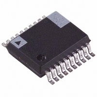
AD6459ARS Analog Devices Inc, AD6459ARS Datasheet - Page 10

AD6459ARS
Manufacturer Part Number
AD6459ARS
Description
IC RCVR IF SUBSYS GSM 3V 20-SSOP
Manufacturer
Analog Devices Inc
Datasheet
1.AD6459ARS.pdf
(12 pages)
Specifications of AD6459ARS
Rohs Status
RoHS non-compliant
Function
Receiver IF Subsystem
Frequency
500MHz
Rf Type
Cellular, GSM, IS-54, TETRA, DCS, PCS
Secondary Attributes
3V, Low Power Receiver IF Subsystem
Package / Case
20-SSOP (0.200", 5.30mm Width)
Operating Temperature (max)
85C
Operating Temperature Classification
Commercial
Operating Supply Voltage (min)
2.7V
Operating Supply Voltage (max)
5.5V
Lead Free Status / Rohs Status
Not Compliant
Available stocks
Company
Part Number
Manufacturer
Quantity
Price
Company:
Part Number:
AD6459ARS
Manufacturer:
AD
Quantity:
1 791
Part Number:
AD6459ARS
Manufacturer:
ADI/亚德诺
Quantity:
20 000
Part Number:
AD6459ARSZ
Manufacturer:
ADI/亚德诺
Quantity:
20 000
AD6459
I/Q Demodulators
Both demodulators (I and Q) receive their inputs internally
from the IF amplifiers. Each demodulator comprises a full-wave
synchronous detector followed by an 8 MHz, two-pole low-pass
filter, producing differential outputs at pins IRXP and IRXN,
and QRXP and QRXN. Using the I and Q demodulators for
IFs above 50 MHz is precluded by the 5 MHz to 50 MHz range
of the PLL used in the demodulator section.
The I and Q outputs are differential and can swing up to
2.2 V p-p at the low supply voltage of 2.7 V. They are nominally
centered at 1.5 V, independent of power supply. They can
therefore directly drive the RX ADCs in the AD7015 baseband
converter, which require an amplitude of 1.23 V to fully load
them when driven by a differential signal. The conversion gain
of the I and Q demodulators is 17 dB.
For IFs of less than 8 MHz, the on-chip low-pass filters (8 MHz
cutoff) do not adequately attenuate the IF or feedthrough
products; thus, the maximum input voltage must be limited to
allow sufficient headroom at the I and Q outputs for not only
the desired baseband signal but also the unattenuated higher-
order demodulation products. These products can be removed
by an external low-pass filter. A simple 1-pole RC filter with its
corner above the modulation bandwidth is sufficient to attenu-
ate undesired outputs. The design of the RC filter is eased by
the 4.7 k resistor integrated at each I and Q output pin.
Phase-Locked Loop
The demodulators are driven by quadrature signals that are
provided by a variable-frequency quadrature oscillator (VFQO),
phase-locked to a reference signal applied to pin FREF. When
this signal is at the IF, inphase and quadrature baseband
outputs are generated at the I output (IRXP and IRXN) and Q
output (QRXP and QRXN), respectively. The quadrature
accuracy of this VFQO is typically within 1.5 at 19.5 MHz. A
simplified diagram of the FREF input is shown in Figure 25.
The VFQO operates from 5 MHz to 50 MHz and is controlled
by the voltage between VPOS and FLTR. In normal operation a
series RC network, forming the PLL loop filter, is connected
from FLTR to V
ensures that the frequency-control voltage on pin FLTR remains
held during power-down, so reacquisition of the carrier occurs
in less than 80 s.
In practice, the probability of a phase mismatch at power-up is
high, so the worst case linear settling period to full lock needs to
be considered in making filter choices. This is typically < 80 s for
a quadrature phase error of
Figure 25. Simplified Schematic of the FREF interface
FREF
POS
. The use of an integral sample-hold system
20k
5k
3 at an IF of 19.5 MHz. Note that
50µA PTAT
5k
V
POS
–10–
the VFQO always provides quadrature between its own I and Q
outputs, but the phasing between it and the reference carrier
will swing around the final value during the PLL’s settling time.
Bias System
The AD6459 operates from a single supply (V
at a typical supply current of 8 mA at midgain and T
corresponding to a power consumption of 24 mW. Any voltage
from 2.7 V to 5.5 V may be used.
The bias system includes a fast-acting active high CMOS-
compatible power-up switch, allowing the part to idle at 2 A
when disabled. Biasing is generally proportional-to-absolute-
temperature (PTAT) to ensure stable gain with temperature.
Other special biasing techniques are used to ensure very
accurate gain, stable over the full temperature range.
USING THE AD6459
In this section, we will focus on a few areas of special impor-
tance and include a few general application tips. As with any
wideband high gain component, great care is needed in PC
board layout. The location of the particular grounding points
must be considered with due regard to the possibility of
unwanted signal coupling.
The high sensitivity of the AD6459 leads to the possibility that
unwanted local EM signals may have an effect on the perfor-
mance. During system development, carefully-shielded test
assemblies should be used. The best solution is to use a fully
enclosed box enclosing all components with the minimum
number of needed signal connectors (RF, LO, I and Q outputs)
in miniature coax form.
Gain Distribution
As with all receivers, the most critical decisions in effectively
using the AD6459 relate to the partitioning of gain between the
various subsections (Mixer, IF Amplifier/Demodulator) and the
placement of filters to achieve the highest overall signal-to-noise
ratio and lowest intermodulation distortion.
Figure 26 shows an example of the main RF/IF signal path at
maximum and minimum signal levels.
Figure 26. Signal Levels and Gain, Showing 76 dB Typical
and 80 dB Maximum Range in an Example Application
SIGNAL LEVEL
–100
–10
–20
–30
–40
–50
–60
–70
–80
–90
IN dBm
IF INPUT
250 MHz
–15dBm
–19dBm
–95dBm
–99dBm
CONVERSION
MIXER
GAIN
–19dBm
–22dBm
–79dBm
–82dBm
FILTER GAIN
3dB
–16dBm
–19dBm
–76dBm
–79dBm
GAIN
IF
–36dBm
POS
DEMOD.
CONV.
) usually 3 V,
GAIN
A
= +25 C,
35mV
CONSTANT
BASEBAND
OUTPUT
REV. 0
Q
I


