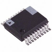
AD6459ARS Analog Devices Inc, AD6459ARS Datasheet - Page 9

AD6459ARS
Manufacturer Part Number
AD6459ARS
Description
IC RCVR IF SUBSYS GSM 3V 20-SSOP
Manufacturer
Analog Devices Inc
Datasheet
1.AD6459ARS.pdf
(12 pages)
Specifications of AD6459ARS
Rohs Status
RoHS non-compliant
Function
Receiver IF Subsystem
Frequency
500MHz
Rf Type
Cellular, GSM, IS-54, TETRA, DCS, PCS
Secondary Attributes
3V, Low Power Receiver IF Subsystem
Package / Case
20-SSOP (0.200", 5.30mm Width)
Operating Temperature (max)
85C
Operating Temperature Classification
Commercial
Operating Supply Voltage (min)
2.7V
Operating Supply Voltage (max)
5.5V
Lead Free Status / Rohs Status
Not Compliant
Available stocks
Company
Part Number
Manufacturer
Quantity
Price
Company:
Part Number:
AD6459ARS
Manufacturer:
AD
Quantity:
1 791
Part Number:
AD6459ARS
Manufacturer:
ADI/亚德诺
Quantity:
20 000
Part Number:
AD6459ARSZ
Manufacturer:
ADI/亚德诺
Quantity:
20 000
The output of the mixer is differential. The nominal conversion
gain is specified for operation into a 19.5 MHz LC IF bandpass
filter as shown in Figure 21 and Table I.
The conversion gain is measured between the mixer input and
the input of this filter and varies between –5 dB and +15 dB.
Frequency
13 MHz
19.5 MHz
26 MHz
40 MHz
The maximum permissible signal level between MXOP and
MXOM is determined by the maximum gain control voltage.
The mixer output port, having pull-up resistors of 250
V
IF Amplifier
Most of the gain in the AD6459 is provided by the IF amplifier
strip, which comprises two stages. Both are fully differential and
each has a gain span of 26 dB for the AGC voltage range of 0.2
V to 2.25 V. Thus, in conjunction with the variable gain of the
mixer, the total gain span is 76 dB. The overall IF gain varies
from –13 dB to 45 dB for the nominal AGC voltage of 0.2 V to
2.25 V. Maximum gain is at V
The IF input is differential, at IFIP and IFIM. Figure 23 shows
a simplified schematic of the IF interface modeled as parallel
RC network.
The IF’s small-signal bandwidth is approximately 50 MHz from
IFIP and IFIM through the demodulator.
REV. 0
POS
Table I. Filter Component Values for Selected Frequencies
Figure 23. IF Amplifier Port Modeled as a Parallel RC
Network
Figure 21. Suggested IF Filter Inserted Between the
Mixer’s Output Port and the Amplifier’s Input Port
, is shown in Figure 22.
V
POS
Figure 22. Mixer Output Port
MXOM
MXOP
IFLO
IFHI
C1
27 pF
27 pF
22 pF
22 pF
250
250
C1
C1
C2
GAIN
C
= 0.2 V.
SH
L1
L1
0.82 H
0.56 H
0.39 H
0.12 H
R
SH
MXOP
MXOM
IFIP
IFIM
C2
180 pF
110 pF
82 pF
100 pF
to
–9–
Gain Scaling
The AD6459’s overall gain, expressed in decibels, is linear with
respect to the AGC voltage V
sections is maximum when V
bias is increased to V
of the power supply voltage. The gain of all stages changes
simultaneously. The AD6459’s gain scaling is also tempera-
ture compensated.
Note that GAIN pin of the AD6459 is an input driven by an
external low impedance voltage source, normally a DAC, under
the control of the radio’s digital processor.
The gain-control scaling is directly proportional to the reference
voltage applied to the pin GREF and is independent of the
power supply voltage. When this input is set to the nominal
value of 1.2 V, the scale is nominally 27 mV/dB (37 dB/V).
Under these conditions, 76 dB of gain range (mixer plus IF)
corresponds to a control voltage of 0.2 V V
The final centering of this 2.05 V range depends on the inser-
tion losses of the IF filters used.
Pin GREF can be tied to an external voltage reference (V
provided, for example, by an AD1580 (1.21 V) voltage reference.
When using the Analog Devices AD7013 (IS54, TETRA, and
satellite receiver applications) and AD7015 or AD6421 (GSM,
DCS1800, PCS1900) baseband converters, the external refer-
ence may also be provided by the reference output of the
baseband converters. The interface between the AD6459 and
the AD6421 baseband converter is shown in Figure 24. The
AD7015 baseband converter provides a V
iary DAC in the AD7015 can be used to generate the AGC
voltage. Since it uses the same reference voltage, the numerical
input to this DAC provides an accurate RSSI value in digital
form, no longer requiring the reference voltage to have high
absolute accuracy.
Figure 24. Interfacing the AD6459 to the AD6421
Baseband Converter
AD6459
QRXP
QRXP
GREF
FREF
GAIN
IRXN
IRXP
GAIN
100pF
100pF
1nF
= 2.25 V. The gain is independent
GAIN
GAIN
VCTCXO
160
0.1µF
is 0.2 V and falls off as the
at pin GAIN. The gain of all
100pF
100pF
R
IRXP
IRXP
IRXP
IRXN
BREFOUT
BREFCAP
AGC DAC
AFC DAC
of 1.23 V. An auxil-
GAIN
AD6421
AD6459
2.25 V.
REF
)


