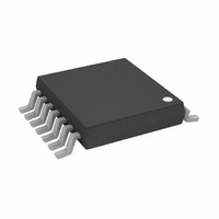
AD8343ARUZ Analog Devices Inc, AD8343ARUZ Datasheet - Page 22

AD8343ARUZ
Manufacturer Part Number
AD8343ARUZ
Description
IC MIXER ACTIVE HI-IP3 14-TSSOP
Manufacturer
Analog Devices Inc
Series
AD8343r
Datasheet
1.AD8343ARUZ.pdf
(32 pages)
Specifications of AD8343ARUZ
Frequency
0Hz ~ 2.5GHz
Rf Type
Cellular, WLAN
Number Of Mixers
1
Gain
7dB
Noise Figure
14dB
Secondary Attributes
Up/Down Converter
Current - Supply
60mA
Voltage - Supply
4.5 V ~ 5.5 V
Package / Case
14-TSSOP (0.173", 4.40mm Width)
Supply Voltage Range
4.5V To 5.5V
Rf Ic Case Style
TSSOP
No. Of Pins
14
Operating Temperature Range
-40°C To +85°C
Msl
MSL 1 - Unlimited
Ic Function
IF Subsystem
Termination Type
SMD
Supply Voltage Min
4.5V
Rohs Compliant
Yes
Operating Temperature (min)
-40C
Operating Temperature (max)
85C
Operating Temperature Classification
Industrial
Filter Terminals
SMD
Digital Ic Case Style
TSSOP
Lead Free Status / RoHS Status
Lead free / RoHS Compliant
Lead Free Status / RoHS Status
Lead free / RoHS Compliant, Lead free / RoHS Compliant
Available stocks
Company
Part Number
Manufacturer
Quantity
Price
Company:
Part Number:
AD8343ARUZ
Manufacturer:
ANALOGDE
Quantity:
2 035
Part Number:
AD8343ARUZ
Manufacturer:
ADI/亚德诺
Quantity:
20 000
AD8343
For the device input, capacitive common-mode loading tends to
produce an unstable circuit, particularly at low frequencies (see
Figure 61). Fortunately, either type of single-ended-to-differential
conversion (transmission line balun or flux-coupled transformer)
tends to produce inductive loading, although some matching
network topologies and/or component values circumvent this
desirable behavior. In general, a simulation of the common-
mode termination seen by the AD8343’s input port is plotted
against the input stability circles to check stability. This is
especially recommended if the single-ended-to-differential
conversion is done with a discrete component circuit.
LOCAL OSCILLATOR INPUT INTERFACE
(LOIP, LOIM)
The LO terminals of the AD8343 are internally biased;
connections to these terminals should include dc blocks,
except as noted below in the DC Coupling the LO section.
The differential LO input return loss (with a 50 Ω differential
input impedance) is presented in Figure 64. As shown, this port
has a typical differential return loss of better than 9.5 dB (2:1 V
SWR). If better return loss is desired for this port, differential
matching techniques can also be applied.
At low LO frequencies, it is reasonable to drive the AD8343
with a single-ended LO, connecting the undriven LO pin to
GND through a dc block. This results in an LO input imped-
ance closer to 25 Ω at low frequencies, which should be factored
into the design. At higher LO frequencies, differential drive is
strongly recommended.
The suggested minimum LO power level is about –12 dBm.
This can be seen in Figure 65.
–10
–15
–20
–25
–30
–5
0
0
Figure 64. LO Input Differential Reflection Coefficient
500
FREQUENCY (50MHz TO 2500MHz)
1000
1500
2000
2500
Rev. B | Page 22 of 32
DC COUPLING THE LO
The AD8343’s LO limiting amplifier chain is internally
dc-coupled. In some applications or experimental situations,
it is useful to exploit this property. Following is the recom-
mended way to do so.
The LO pins are internally biased at about 360 mV with respect
to COMM. Driving the LO to either extreme requires injecting
several hundred microamps into one LO pin and extracting
about the same amount of current from the other. The incre-
mental impedance at each pin is about 25 Ω, so the voltage level
on each pin is disturbed very little by the application of external
currents in that range.
Figure 66 illustrates how to drive the LO port with continuous
dc and also from standard ECL powered by –5.2 V.
–5.2V
ECL
5
4
3
2
1
0
–5.2V
–5.2V
–40
3.6kΩ
390Ω
390Ω
1.2kΩ
Figure 65. Gain and Noise Figure vs. LO Input Power
13kΩ
1.2kΩ
1kΩ
+5V
Figure 66. DC Interfaces to the LO Port
3.6kΩ
10
10
4
6
9
4
6
9
–30
DCPL
DCPL
PWDN
PWDN
LOIM
LOIM
LOIP
LOIP
VPOS
VPOS
LO POWER (dBm)
5
DRIVER
5
DRIVER
BIAS
BIAS
LO
LO
1
1
–20
7
7
COMM
INPUT RF = 900MHz
OUTPUT IF = 170MHz
LO LOW SIDE INJECTION
CONVERSION GAIN
8
8
NOISE FIGURE
COMM
11
11
2
2
14
14
INPP
INPP
–10
AD8343
AD8343
3
3
INPM
INPM
25
20
15
10
5
0
13
12
13
12


