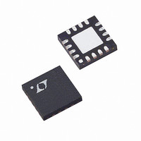
LT5512EUF Linear Technology, LT5512EUF Datasheet - Page 10

LT5512EUF
Manufacturer Part Number
LT5512EUF
Description
IC MIXER DWNCONV HI SIGN 16-QFN
Manufacturer
Linear Technology
Series
LT5512r
Datasheet
1.LT5512EUF.pdf
(12 pages)
Specifications of LT5512EUF
Rf Type
Cellular, HF, ISM, PCS, UHF, VHF, WMTS
Frequency
1kHz ~ 3GHz
Number Of Mixers
1
Gain
1.1dB
Noise Figure
14dB
Secondary Attributes
Down Converter
Current - Supply
74mA
Voltage - Supply
4.5 V ~ 5.25 V
Package / Case
16-WQFN Exposed Pad
Operating Temperature (min)
-40C
Operating Temperature (max)
85C
Operating Temperature Classification
Industrial
Lead Free Status / RoHS Status
Contains lead / RoHS non-compliant
Available stocks
Company
Part Number
Manufacturer
Quantity
Price
Part Number:
LT5512EUF
Manufacturer:
LINEAR/凌特
Quantity:
20 000
Part Number:
LT5512EUF#PBF
Manufacturer:
LINEAR/凌特
Quantity:
20 000
Company:
Part Number:
LT5512EUF#TRPBF
Manufacturer:
SP
Quantity:
5 997
Part Number:
LT5512EUF#TRPBF
Manufacturer:
LINEAR/凌特
Quantity:
20 000
APPLICATIO S I FOR ATIO
LT5512
impedance and differential refl ection coeffi cient between
the LO
compute the value of the series matching inductor, L3.
Alternatively, Figure 8 shows measured LO input return
loss versus frequency for various values of L3. Reactive
LO port matching is used on the high-frequency evaluation
board (see Figure 2).
IF Output Port
The differential IF outputs, IF
nected to the collectors of the mixer switching transistors
as shown in Figure 9. These outputs should be combined
externally through an RF balun or 180° hybrid to achieve
optimum performance. Both pins must be biased at the
supply voltage, which can be applied through matching
inductors (see Figure 2), or through the center-tap of an
output transformer (see Figure 1). These pins are protected
with ESD diodes; the diodes allow peak AC signal swing
up to 1.3V above V
As shown in Table 3, the IF output differential impedance
is approximately 390Ω in parallel with 0.44pF. A simple
band-pass IF matching network suitable for wireless ap-
plications is shown in Figure 9. Here, L1, L2 and C3 set the
desired IF output frequency. The 390Ω differential output
can then be applied directly to a differential fi lter, or an
8:1 balun for impedance transformation down to 50Ω.
To achieve maximum linearity, C3 should be located as
10
+
Figure 8. Single-Ended LO Port Return Loss
and LO
vs Frequency for Various Values of L3
–20
–25
–30
–10
–15
–5
0
0
–
500
pins. This information can be used to
CC
U
1000
.
FREQUENCY (MHz)
1500
U
10nH
2000 2500
8.2nH
+
6.8nH
and IF
5.6nH
4.7nH
W
3000 3500 4000
–
, are internally con-
1573 F08
U
close as possible to the IF
of inductance in series with C3 (such as through a via)
can signifi cantly degrade IIP3. The value of C3 should be
reduced by the value of internal capacitance (see Table 3).
This matching network is simple and offers good selectivity
for narrow band IF applications.
For IF frequencies below 100MHz, the simplest IF matching
technique is an 8:1 transformer connected across the IF
pins as shown in Figure 1. DC bias to the IF
is provided through the transformer’s center-tap. A small
value IF capacitor (C3) improves the LO-IF leakage and
attenuates the undesired image frequency. No inductors
are required.
Table 3. IF Output Differential Impedance (Parallel Equivalent)
Frequency
(MHz)
1000
1250
1500
1900
170
240
450
750
860
10
70
Figure 9. IF Output Equivalent Circuit
with Band-Pass Matching Elements
Differential Output
LT5512
394 II - j5445
393 II - j2112
392 II - j1507
400Ω
396 II - j10k
387 II - j798
377 II - j478
371 II - j416
363 II - j359
363 II - j295
317 II - j192
Impedance
346 II -j244
11
10
+
/IF
IF
C3
IF
+
–
–
pins. Even small amounts
L1
L2
0.766
0.775
0.774
0.773
0.772
0.768
0.766
0.762
0.764
0.756
0.743
Mag
5512 F09
V
Differential S11
CC
TO
DIFFERENTIAL
FILTER OR
BALUN
+
and IF
Angle
–12.2
–14.0
–16.2
–19.6
–23.6
–29.9
–1.1
–2.8
–3.9
–7.3
–
0
pins
5512fa


